Process for manufacturing cavity of package substrate

A manufacturing process and a technology for packaging substrates, which are used in semiconductor/solid-state device manufacturing, electrical components, circuits, etc., and can solve the problems of difficult removal of solder resist ink, scratches on wire gold fingers, and low cavity yield rate, and improve the Process production efficiency, improve quality, and eliminate the effect of cumbersome operations

Inactive Publication Date: 2014-04-16
SHENNAN CIRCUITS
View PDF4 Cites 6 Cited by
  • Summary
  • Abstract
  • Description
  • Claims
  • Application Information

AI Technical Summary

Problems solved by technology

There are controlled deep milling steps in the manufacturing process of the cavity, and the use of controlled deep milling steps will cause scratches on the wire bonding gold fingers
In order to protect the wire bonding gold fingers, the industry generally uses solder resist ink to cover the wire bonding gold fingers, and then removes the solder resist ink in the subsequent process, but the solder resist ink is very difficult to remove, resulting in low cavity yield, cumbersome operation, and long production cycle. question

Method used


Image

  • Process for manufacturing cavity of package substrate
  • Process for manufacturing cavity of package substrate
  • Process for manufacturing cavity of package substrate

Examples


Embodiment Construction

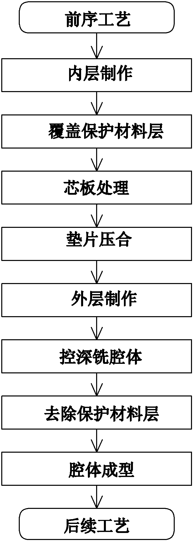
[0030] It should be noted that, in the case of no conflict, the embodiments in the present application and the features in the embodiments can be combined with each other. The present invention will be further described in detail below in conjunction with the drawings and specific embodiments. This embodiment is based on Figure 7 The direction shown prevails.

[0031] Such as Figure 1 to Figure 7 As shown, the embodiment of the present invention provides a manufacturing process of a packaging substrate cavity, including the following steps:

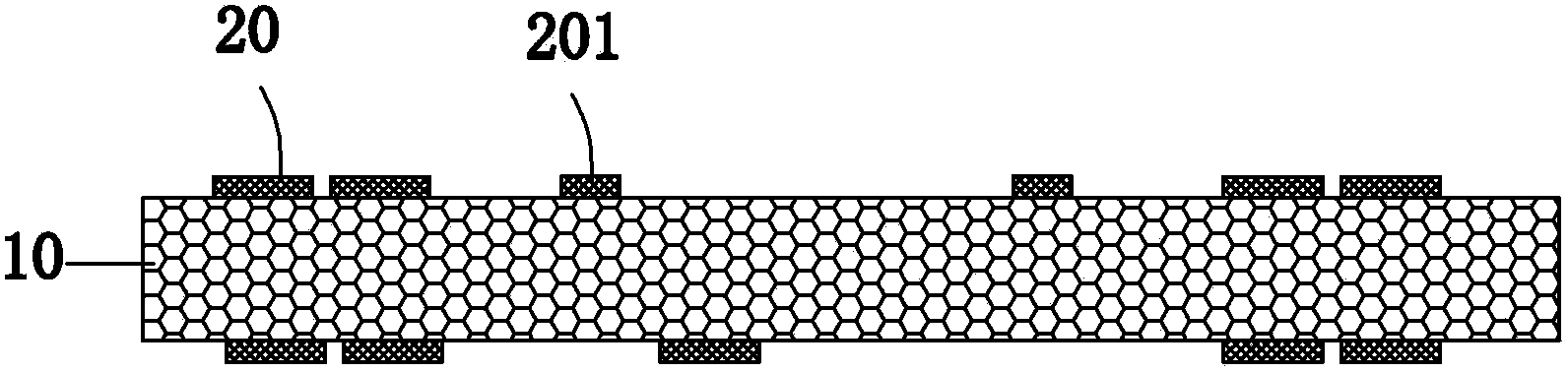
[0032] Making the inner layer: making the required circuit layer 20 on the core board 10;

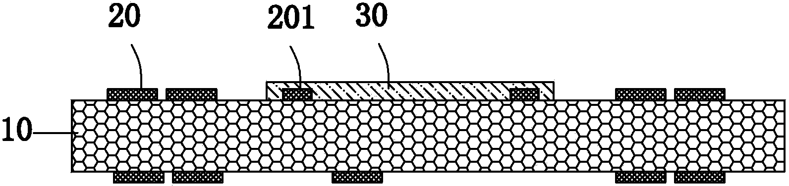
[0033] Covering the protective material layer: determine the target cavity area on the core board 10 after the inner layer is completed, and cover the protective material layer 30 above the wire bonding gold finger 201 in the target cavity area, so that the wire bonding gold finger 201 is covered by the protective material layer 30 full coverag...


PUM


Abstract

The embodiment of the invention discloses a process for manufacturing a cavity of a package substrate. The process includes the following steps that an inner layer is manufactured; a protective material layer is laid, namely, a target cavity zone is determined on a core board with the inner layer manufactured, and a bonding golden finger of the target cavity zone is covered with the protective material layer; the core board is treated; the protective material layer is overlaid with a gasket in a press fit mode; an outer layer is manufactured; cavity depth-control milling is carried out, namely, depth-control milling is carried out on the target cavity zone of the core board with the outer layer manufactured to obtain a semi-finished cavity and expose the protective material layer; the protective material layer is removed, and namely the protective material layer in the semi-finished cavity is removed through the organic stripping method to expose the bonding golden finger; cavity forming is carried out, and namely the core board and the interior of the semi-finished cavity with the protective material layer removed are treated through the surface treatment method to obtain the formed cavity. According to the process for manufacturing the cavity of the package substrate, damage to the bonding golden finger is avoided, the dimensional accuracy and quality of the cavity are guaranteed, and the efficiency of the manufacturing process is improved.

Description

technical field [0001] The invention relates to the field of PCB board production, in particular to a manufacturing process of a packaging substrate cavity. Background technique [0002] With the trend of packaging substrates becoming smaller and thinner, it is required that the arrangement of gold wires between the packaging substrate and the chip be denser, resulting in the fabrication of the cavity structure of the packaging substrate. During the conduction process between the chip and the package substrate, the inner gold fingers can be used for bonding. The so-called bonding is the client-side Bonding (bonding) welding, commonly known as bonding. There are controlled deep milling steps in the manufacturing process of the cavity, and the use of controlled deep milling steps will cause scratches on the wire bonding gold fingers. In order to protect the wire bonding gold fingers, the industry generally uses solder resist ink to cover the wire bonding gold fingers, and the...

Claims


Application Information

Patent Timeline
Patent Type & Authority Applications(China)
IPC IPC(8): H01L21/48
CPCH01L21/4867
Inventor 高成志杨家雄郑仰存
Owner SHENNAN CIRCUITS
Why Eureka
Try Eureka