Piece drawing device for semiconductor visual inspection machine

A technology for visual inspection machines and semiconductors, which is applied in semiconductor/solid-state device manufacturing, conveyor objects, transportation and packaging, etc. Easy to drop, prolonging the service life

Inactive Publication Date: 2014-04-16
CHENGDU ADVANCED POWER SEMICON +1
View PDF5 Cites 0 Cited by
  • Summary
  • Abstract
  • Description
  • Claims
  • Application Information

AI Technical Summary

Problems solved by technology

[0005] In the drawing kit, the sliding mounting block in the prior art has the following technical problems: because the sliding mounting block is used more frequently, it is designed as a marble-shaped slider. effective sliding
[0008] Wears out over time, preventing jaws from fully closing when closing
When the frame is pulled out, the frame cannot be clamped stably, and the frame cannot be sent to the designated p

Method used


Image

  • Piece drawing device for semiconductor visual inspection machine
  • Piece drawing device for semiconductor visual inspection machine
  • Piece drawing device for semiconductor visual inspection machine

Examples


Example Embodiment

[0040] The present invention will be further described in detail below in combination with test examples and specific implementations. However, it should not be understood that the scope of the above-mentioned subject of the present invention is limited to the following embodiments, and all technologies implemented based on the content of the present invention belong to the scope of the present invention.
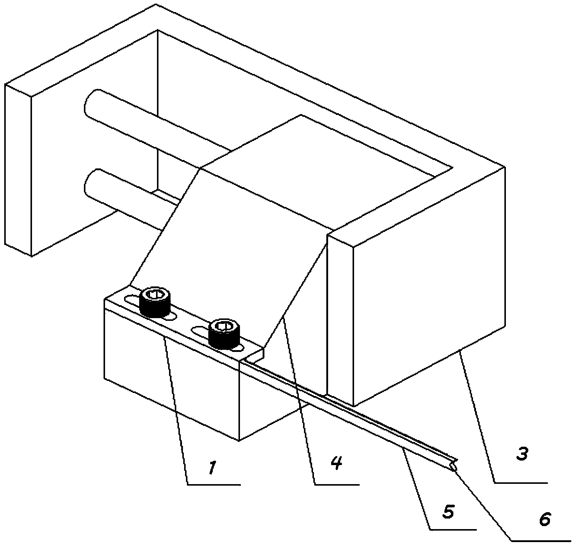
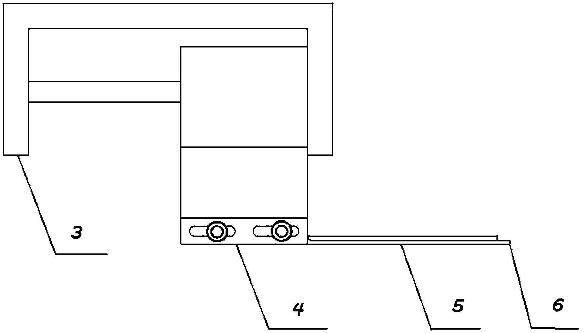
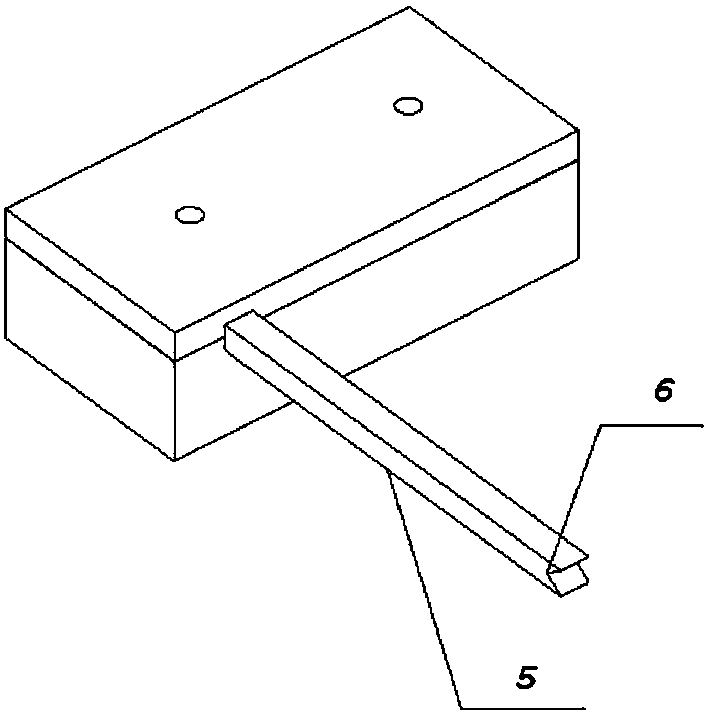
[0041] A piece drawing device of a semiconductor visual inspection machine, comprising a piece drawing kit and a claw kit, such as figure 1 , figure 2 with image 3 As shown, the extraction kit 1 includes a driving rod, a mounting base 3, a sliding rod, a sliding mounting block 4, and a feeding push rod 5. The mounting base 3 is arranged on the driving rod, The sliding mounting block is connected to the mounting base through a sliding rod and a spring, The feeding push rod 5 is connected with the sliding mounting block 4;

[0042] The piece extraction kit 1 further includes...


PUM

PropertyMeasurementUnit
Thicknessaaaaaaaaaa
Thicknessaaaaaaaaaa
Widthaaaaaaaaaa

Abstract

The invention relates to a semiconductor packaging inspection device, in particular to a piece drawing device for a semiconductor visual inspection machine. The piece drawing device for the semiconductor visual inspection machine comprises a piece drawing set and a clamping jaw set. The piece drawing set comprises a driving rod, a mounting base, a sliding rod, a sliding mounting block and a feeding push plate. The mounting base is arranged on the driving rod, the sliding mounting block is connected with the mounting base through the sliding rod and a spring, and the feeding push plate is connected with the sliding mounting block. The piece drawing set further comprises a distance sensor induction piece, the distance sensor induction piece is arranged on the mounting base, and the front end of the feeding push plate is provided with a V-shaped groove. A frame can smoothly enter the visual inspection machine from a material box and smoothly return to the material box from the visual inspection machine, and the problem that the frame moving back and forth between the visual inspection machine and the material box is discarded and scrapped due to feeding and blanking, and waste products and product quality risks are caused on the frame is solved.

Description

[0001] technical field [0002] The invention relates to a semiconductor packaging and testing device, in particular to a chip picking device for a semiconductor visual inspection machine. Background technique [0003] In the field of semiconductor packaging and testing devices, specifically in the field of semiconductor visual inspection machine chip extraction devices, there is a semiconductor visual inspection machine chip extraction device in the prior art. Device Kit" and other components are combined. The device is used to visually inspect the semi-finished products in the front section, and send the film to the designated position for visual inspection. At the same time, it can make the frame enter the visual inspection machine from the material box and return the sampling inspection machine to the material box smoothly, so as to realize all round-trip and random inspection. The frame of the machine and the material box does not form a frame discarded and scrapped ...

Claims


Application Information

Patent Timeline
IPC IPC(8): H01L21/677
CPCH01L21/67242
Inventor 王利华胡晶薛振坤
Owner CHENGDU ADVANCED POWER SEMICON
Why Eureka
Try Eureka