Display device and color film substrate and manufacturing method thereof

A technology of color film substrate and manufacturing method, which is applied in nonlinear optics, instruments, optics, etc., and can solve the problems of wide black matrix width, side light leakage, etc.

Inactive Publication Date: 2014-04-23
BEIJING BOE OPTOELECTRONCIS TECH CO LTD
View PDF8 Cites 2 Cited by
  • Summary
  • Abstract
  • Description
  • Claims
  • Application Information

AI Technical Summary

Problems solved by technology

[0008] The purpose of the present invention is to provide a display device, a color filter substrate and a manufacturing method thereof, so as to overcome the defects of the color filter substrate in the prior art, such as wide black matrix width and side light leakage.

Method used


Image

  • Display device and color film substrate and manufacturing method thereof
  • Display device and color film substrate and manufacturing method thereof
  • Display device and color film substrate and manufacturing method thereof

Examples


Embodiment 1

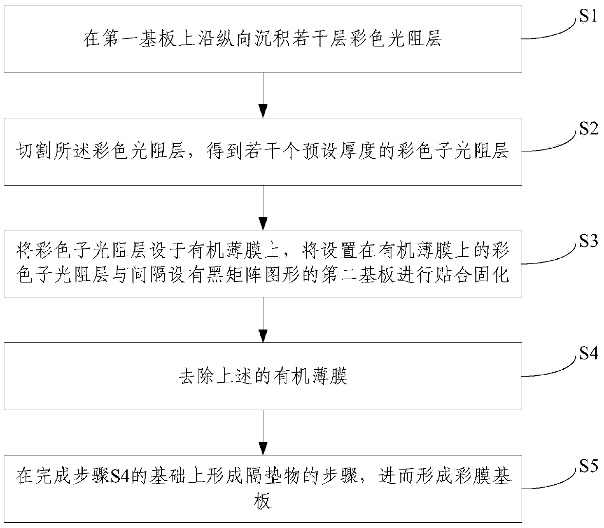
[0035] like Figure 2~3 As shown, the present invention provides a method for manufacturing a color filter substrate, which includes the following steps:

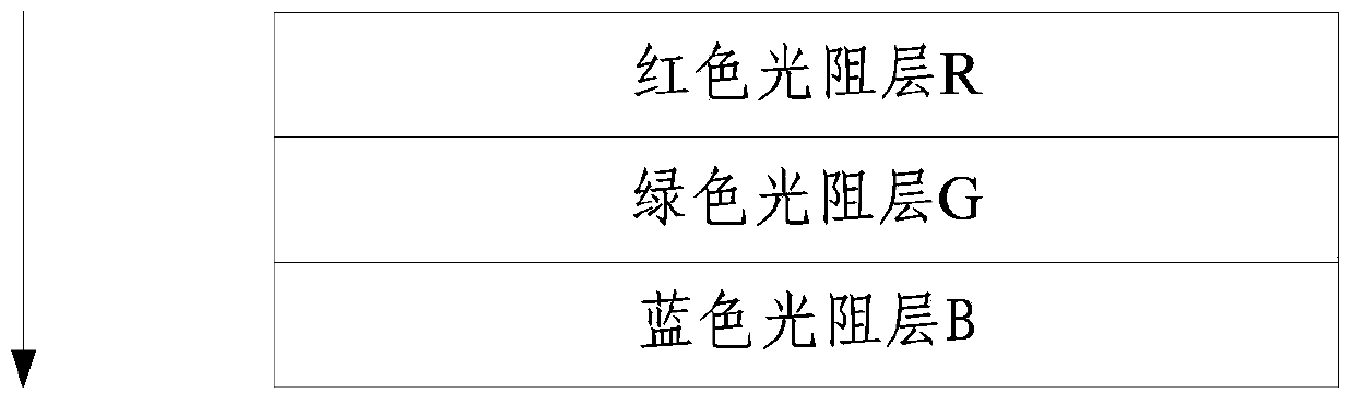
[0036] Step S1, depositing several layers of color photoresist layers on the first substrate 1 along the longitudinal direction;

[0037] Specifically, in this step, the color photoresist layer at least includes a red photoresist layer R, a green photoresist layer G and a blue photoresist layer B. The red photoresist layer R, the green photoresist layer G and the blue photoresist layer B are respectively deposited on the first substrate 1 (such as glass) along the longitudinal direction (in the direction of the arrow), and the deposition order of the colors of the color photoresist layers is not specified. limited.

[0038] In actual production, the photoresist layer can be made of resin material.

[0039] In addition, the thickness of each film layer can be made according to the required pixel size. For example, if the ...

Embodiment 2

[0053] like Figure 5 As shown, the present invention also provides a color filter substrate, including: a first substrate 1, a color photoresist layer arranged laterally adjacent to the first substrate, and the color photoresist layer at least includes a red photoresist layer 2, Blue photoresist layer 3 and green photoresist layer 4;

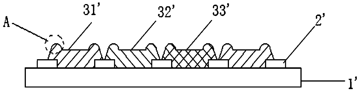
[0054]The second substrate 8 is provided with a black matrix pattern 7, and the first substrate 1 and the second substrate 8 are bonded together. The black matrix 7 is located at the adjacent junction of the color photoresist layers of different colors. location.

[0055] With the color filter substrate of the above structure, there is no space between photoresist layers of different colors, and a black matrix is ​​arranged on the color photoresist layer. Since the black matrix is ​​located above the color photoresist layer, it can play a light-shielding effect on the one hand. On the other hand, the width of the black matrix can be reduced; ...


PUM


Abstract

The invention relates to the technical field of displaying, in particular to a display device and a color film substrate and a manufacturing method thereof. The manufacturing method of the color film substrate includes that a plurality of colorful photoresist layers are vertically deposited on a first substrate, the colorful photoresist layers are cut to obtain a plurality of colorful sub photoresist layers with preset thickness, the colorful sub photoresist layers are arranged on an organic film, the colorful sub photoresist layers arranged on the organic film and a second substrate provided with black matrix patterns at intervals are bonded in a solidifying mode, and the organic film is removed to form the color film substrate. Due to the fact that the colorful sub photoresist layers arranged on the organic film and the substrate provided with the black matrix patterns are bonded in a solidifying mode, a gap-free colorful photoresist layer can be formed, the width requirement of the black matrix is reduced to the largest extent, and light leakage caused by angle section difference is effectively removed.

Description

technical field [0001] The invention relates to the field of display technology, in particular to a display device, a color filter substrate and a manufacturing method thereof. Background technique [0002] In recent years, with the development of science and technology, liquid crystal display technology has also been continuously improved. TFT-LCD (Thin Film Transistor-Liquid Crystal Display, Thin Film Field Effect Transistor-Liquid Crystal Display) occupies an important position in the display field due to its advantages of good image display quality, low energy consumption, and environmental protection. [0003] With the rapid development of display technology, users have higher and higher requirements on the color and brightness of the display screen, and one of the factors affecting the color and brightness is the structural performance of the color filter substrate in the liquid crystal display device. [0004] like figure 1 As shown, it is a schematic structural dia...

Claims


Application Information

Patent Timeline
Patent Type & Authority Applications(China)
IPC IPC(8): G02F1/1335G02F1/1333
Inventor 谢建云车春城
Owner BEIJING BOE OPTOELECTRONCIS TECH CO LTD
Why Eureka
Try Eureka