Supercharge Your Innovation With Domain-Expert AI Agents!

Solid-state image sensor

A solid-state image and sensor technology, applied in the field of solid-state image sensors, can solve problems such as sensitivity variation, and achieve the effect of eliminating sensitivity variation and improving sensitivity

Active Publication Date: 2014-04-30
CANON KK
View PDF9 Cites 6 Cited by
  • Summary
  • Abstract
  • Description
  • Claims
  • Application Information

AI Technical Summary

Problems solved by technology

Also, when the distance between the interface 106f and the radiation reflector 128 is not uniform over the image sensing surface, the amount of photons returning to the photosensor 110 varies, thereby causing sensitivity variations

Method used


Image

  • Solid-state image sensor
  • Solid-state image sensor
  • Solid-state image sensor

Examples


Embodiment Construction

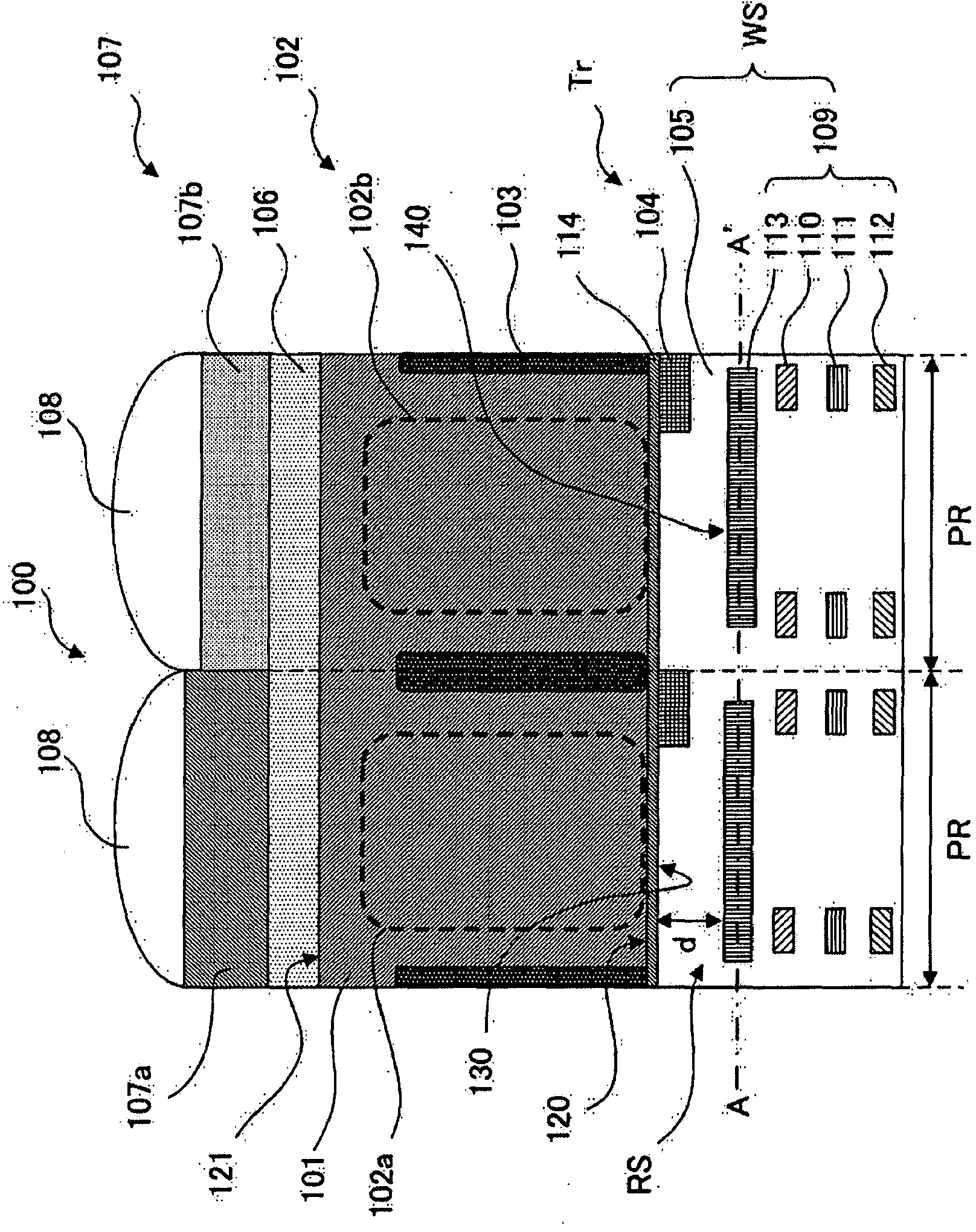
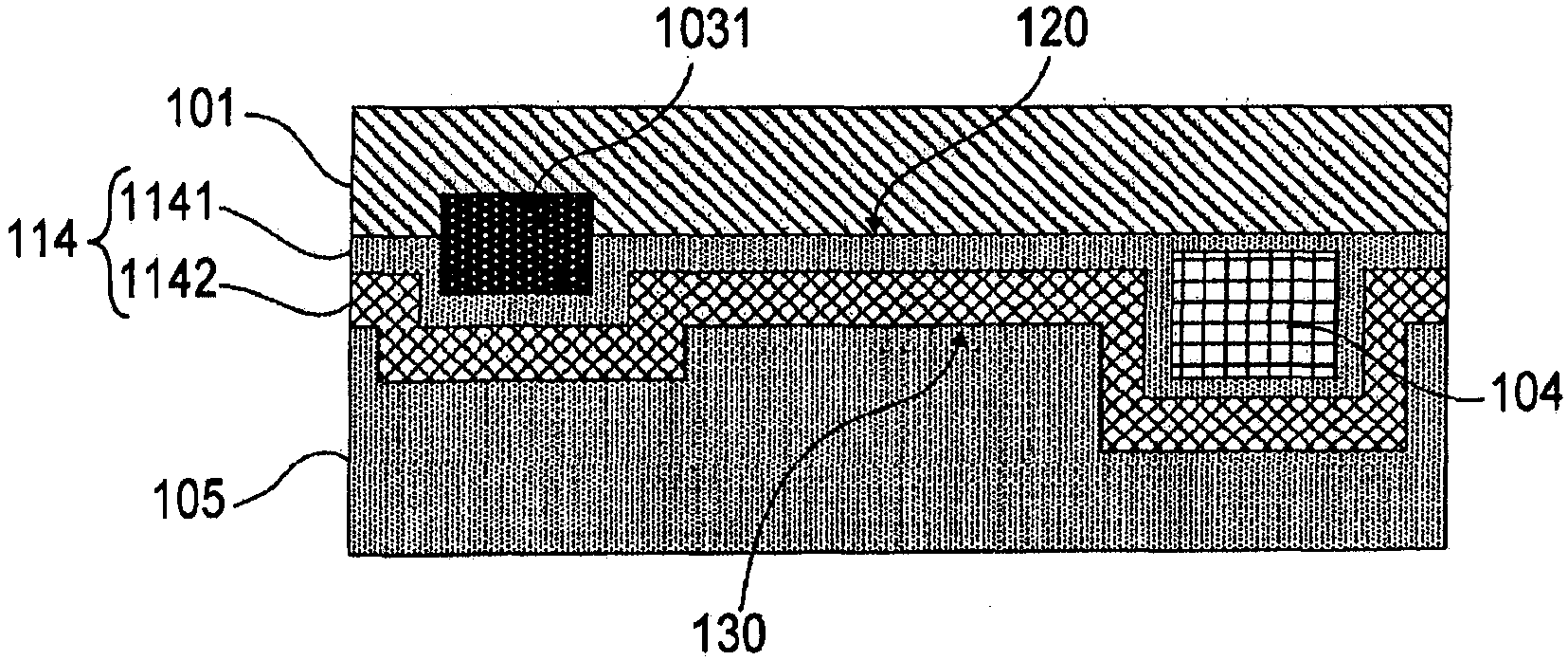
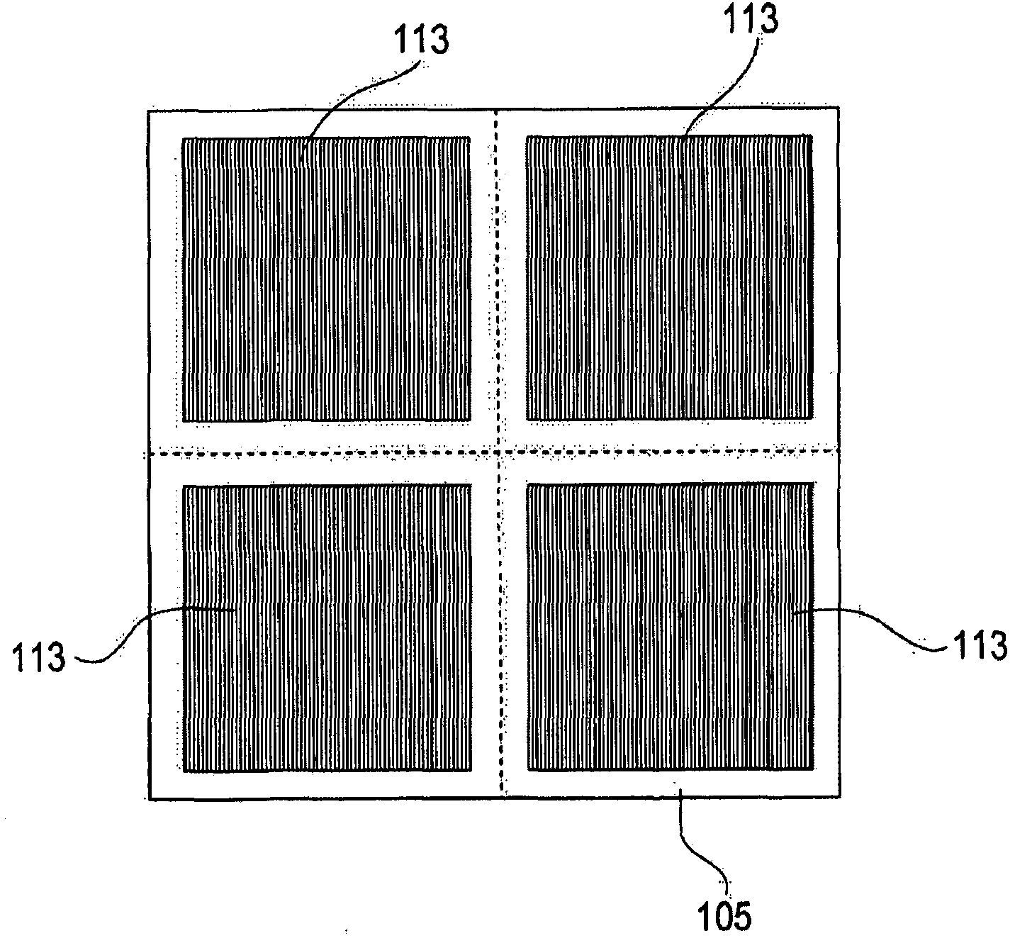
[0015] The following will refer to Figure 1A with 1B as well as Figure 2 to Figure 6 The solid-state image sensor 100 according to the first embodiment of the present invention is described. Figure 1A It is a cross-sectional view of the solid-state image sensor 100 taken along a plane perpendicular to its image sensing surface, and, for the purpose of simplification, only two pixels are shown. Note that the image sensing surface is the surface on which the pixel array is arranged. A pixel array is formed by arranging a plurality of pixels. Figure 1B Is the plane perpendicular to the image sensing surface of the anti-reflection layer 114 of the solid-state image sensor 100 (and Figure 1A Different) an enlarged view of the obtained cross section. figure 2 Is the edge of the solid-state image sensor 100 as a plane parallel to its image sensing surface Figure 1A A cross-sectional view taken from the plane A-A' in. The solid-state image sensor 100 may be configured as, for ex...


PUM


Abstract

A solid-state image sensor includes a semiconductor layer having photoelectric conversion portions, and a wiring structure arranged on a side of a first face of the semiconductor layer, and receives light from a side of a second face of the semiconductor layer. The wiring structure includes a reflection portion having a reflection surface reflecting light transmitted through the semiconductor layer from the second face toward the first face, toward the semiconductor layer, and an insulation film located between the reflection surface and the first face. The sensor includes a first dielectric film arranged to contact the first face, and a second dielectric film arranged between the insulation film and the first dielectric film and having a refractive index different from refractive indices of the first dielectric film and the insulation film.

Description

Technical field [0001] The present invention relates to a solid-state image sensor. Background technique [0002] U.S. Patent No. 7,755,123 describes the rear side irradiated imaging device in which the thickness of the substrate is reduced to allow the photosensor to easily detect light incident on the rear surface. Attached to this manual Figure 8 The rear side illumination imaging device described in FIG. 1C of U.S. Patent No. 7,755,123 is cited. The imaging device described in US Patent No. 7,755,123 includes a radiation reflector 128 that reflects photons incident on the rear surface of the semiconductor device substrate 104 and transmitted through the rear surface of the semiconductor device substrate 104 toward the photosensor 110. [0003] However, with the arrangement described in U.S. Patent No. 7,755,123, the front side 106f, which is the interfacial surface between the semiconductor device substrate 104 and the dielectric layer 118, is reflected toward the radiation re...

Claims


Application Information

Patent Timeline
IPC IPC(8): H01L27/14H01L27/146
CPCH01L27/14621H01L27/1464H01L27/14636H01L27/14629
Inventor 加藤太朗
Owner CANON KK
Features
  • R&D
  • Intellectual Property
  • Life Sciences
  • Materials
  • Tech Scout
  • Unparalleled Data Quality
  • Higher Quality Content
  • 60% Fewer Hallucinations
Learn More