Circuit-board manufacturing method

A circuit board manufacturing and circuit board technology, which is applied in the fields of printed circuit manufacturing, printed circuit, printed circuit assembly of electrical components, etc., can solve problems such as difficult control of processing quality, pollution sources, skewed assembly of components, etc., to avoid waste of high-priced metals, The effect of reducing pollution sources and saving material costs

Inactive Publication Date: 2014-05-07
BOARDTEK ELECTRONICS CORP
View PDF3 Cites 3 Cited by
  • Summary
  • Abstract
  • Description
  • Claims
  • Application Information

AI Technical Summary

Problems solved by technology

[0006] However, the above-mentioned manufacturing method belongs to the subtractive processing technology commonly known in the industry. It not only wastes a lot of high-priced metals in the processing process of different heights, but also consumes more energy and generates a lot of pollution sources due to the repeated execution

Method used


Image

  • Circuit-board manufacturing method
  • Circuit-board manufacturing method
  • Circuit-board manufacturing method

Examples


Embodiment Construction

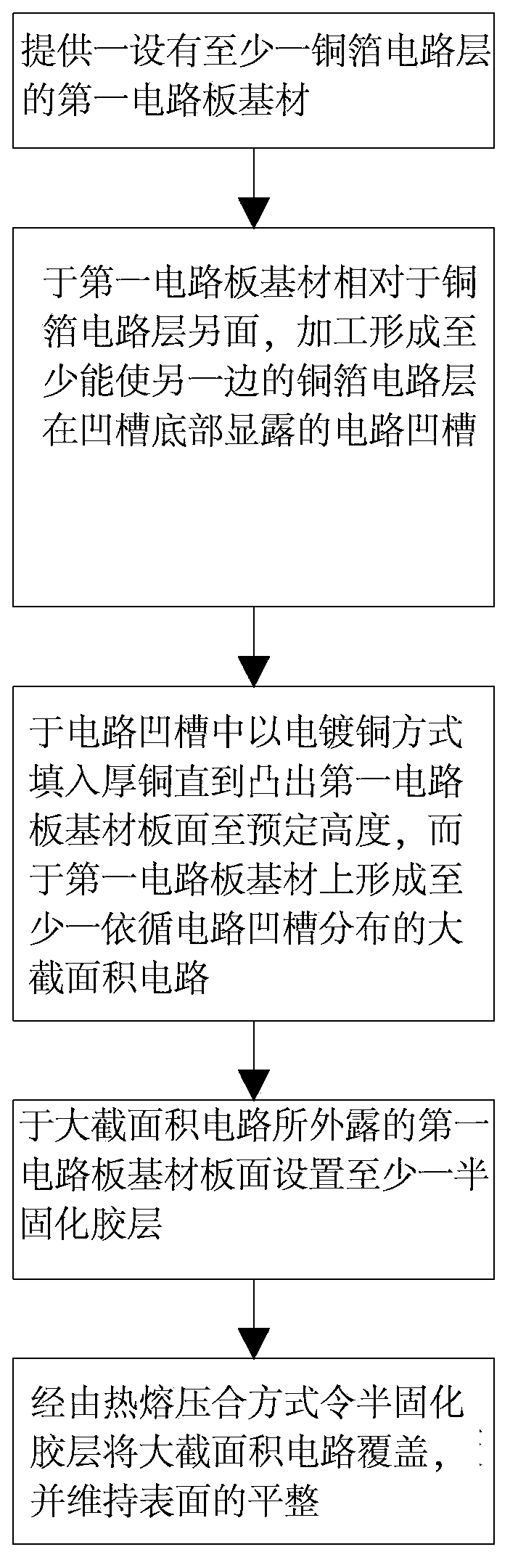
[0052] like figure 1 As shown in the basic flow chart of the present invention, the circuit board manufacturing method of the present invention basically includes the following steps.

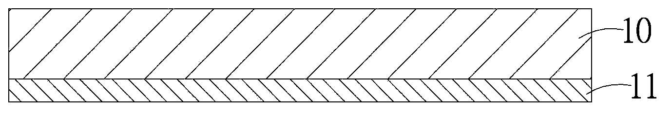
[0053] a. Provide as figure 2 The shown first circuit board substrate 10 is provided with at least one copper foil circuit layer 11; during implementation, the first circuit board substrate 10 may be provided with a copper foil circuit layer 11 on one of its surfaces, or may be provided on two surfaces. Each board surface is provided with a copper foil circuit layer.

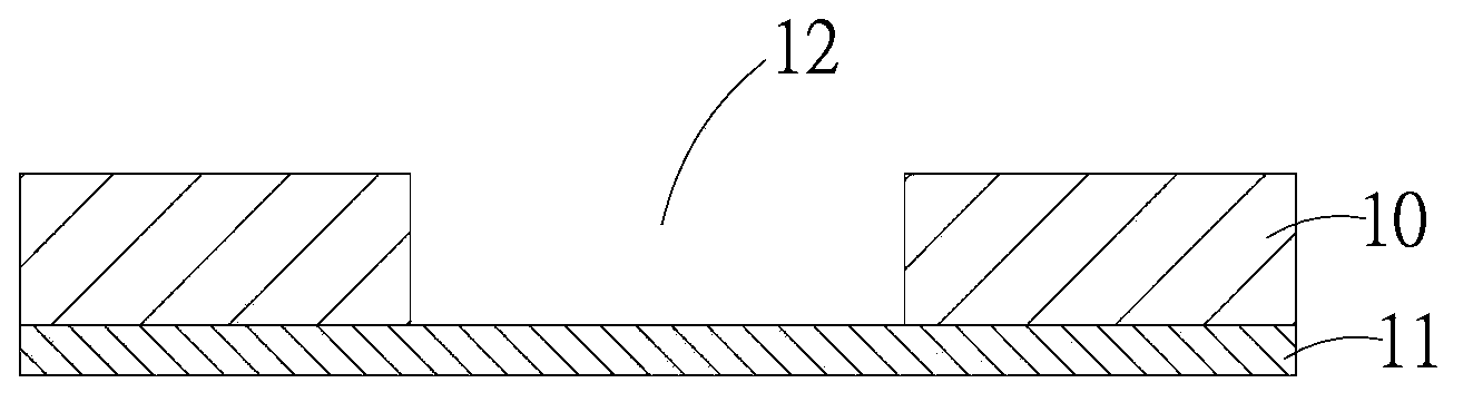
[0054] b. On the other side of the first circuit board substrate 10 relative to the copper foil circuit layer 11 (as shown in the figure, the other side of the first circuit board substrate 10 relative to the copper foil circuit layer 11 ), processing to form at least the The circuit groove 12 of the copper foil circuit layer 11 on the other side is exposed at the bottom of the groove.

[0055] c. If Figure 4 As shown, thic...


PUM


Abstract

The invention discloses a circuit-board manufacturing method and provides a circuit-board manufacturing method capable of manufacturing at least one large-cross-section circuit hidden in a board body on a circuit-board substrate. In the circuit-board manufacturing method, basically on a first circuit-board substrate provided with a copper-foil circuit layer, a circuit groove which is at least capable of making a copper-foil circuit layer at the other side exposed at the bottom part of the groove is formed through processing; then thick copper is filled into the circuit groove in an electrocoppering method until projecting out of the first circuit-board substrate for a preset height and thus the large-cross-section circuit which is distributed along the circuit groove is formed; and then the first circuit-board substrate exposed by the large-cross-section circuit is covered with at least one semi-cured adhesive layer and through a hot-melting laminating method, the semi-cured adhesive layer is made cover the large-cross-section circuit and flatness of the surface is maintained so that a circuit board, in which at least one thin circuit and least one large-cross-section circuit can be manufactured on the same first circuit-board substrate, can be obtained. Therefore, objectives of saving material cost, preventing waste of high-price metals and reducing pollution sources are achieved.

Description

technical field [0001] The present invention relates to the circuit fabrication technology of printed boards, in particular to a circuit board fabrication method that is particularly suitable for fabricating at least one thin circuit and at least a large cross-sectional area circuit on the same circuit board substrate. Background technique [0002] As we all know, the printed circuit board (Printed Circuit Board, PCB) plays the circuit connection between the various electronic components by the circuit layer (copper film) that transmits the telecommunication, and integrates the required circuit net into the plane and distributes it on the surface of the printed circuit board or Three-dimensional circuit layers to form a network of connections between components at different positions. [0003] In principle, the basic materials of general printed circuit boards (hereinafter collectively referred to as substrates) are mostly laminates made of insulating paper, glass fiber clot...

Claims


Application Information

Patent Timeline
IPC IPC(8): H05K3/18H05K3/36
Inventor 李建成
Owner BOARDTEK ELECTRONICS CORP
Why Eureka
Try Eureka