Circuit board and manufacturing method thereof

A technology of circuit boards and graphics, which is applied in the fields of printed circuit manufacturing, printed circuits, printed circuit components, etc., can solve the problems of leakage, increased risk of abnormal boards, and low production efficiency, so as to prevent missed inspections, reduce manpower consumption, The effect of improving productivity

Inactive Publication Date: 2016-12-21
AVARY HLDG (SHENZHEN) CO LTD +1
View PDF3 Cites 0 Cited by
  • Summary
  • Abstract
  • Description
  • Claims
  • Application Information

AI Technical Summary

Problems solved by technology

When the pads are dense, it is very labor-intensive to manually check whether the solder resist ink on the product is printed on the pads one by one, and there are often leakages, which makes the production efficiency low and increases the risk of abnormal boards flowing into the client

Method used


Image

  • Circuit board and manufacturing method thereof
  • Circuit board and manufacturing method thereof
  • Circuit board and manufacturing method thereof

Examples


Embodiment Construction

[0015] The circuit board provided by the technical solution and its manufacturing method will be further described in detail below in conjunction with the accompanying drawings and embodiments.

[0016] The manufacturing method of the circuit board provided by the embodiment of the technical solution includes the following steps:

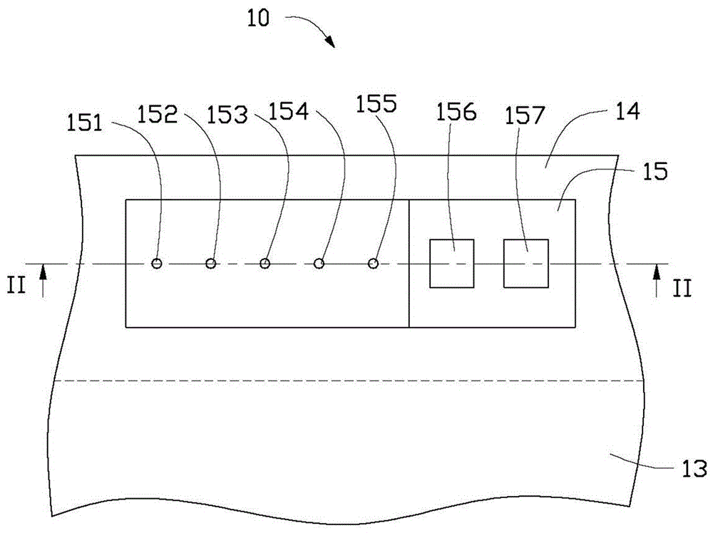
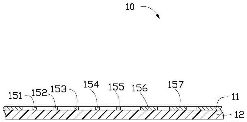
[0017] For a first step, see Figure 1-2 , a circuit substrate 10 is provided.

[0018] In this embodiment, a single-sided circuit substrate 10 is taken as an example for illustration. The circuit substrate 10 includes a conductive circuit layer 11 and an insulating layer 12 .

[0019] The conductive circuit layer 11 and the insulating layer 12 are made of commonly used materials for circuit boards. For example, the material of the conductive circuit layer 11 can be copper, silver, tin, etc.; the material of the insulating layer 12 can be pure resin such as epoxy resin, polyimide resin, etc., or a resin containing reinforcing materials. Such as ...


PUM


Abstract

Provided is a circuit board equipped with a product portion and a non-product portion except the product portion. A solder mask layer is formed on the product portion. The non-product portion comprises a testing area in which multiple solder mask figures and multiple bonding pads are formed. Each solder mask figure is in an annular shape and corresponds and surrounds a bonding pad. The inner edge line of each solder mask figure is far from the bonding pad corresponding to the solder mask figure. The invention also provides a method for manufacturing the above circuit board.

Description

technical field [0001] The invention relates to circuit board detection technology, in particular to a circuit board printed with solder resist ink and a manufacturing method of the circuit board printed with solder resist ink. Background technique [0002] In the circuit board manufacturing process, in order to protect the circuit layer on the outer layer of the circuit board, solder resist ink is usually printed on the outer layer of the circuit board. Generally, a plurality of pads are arranged on the circuit layer of the outer layer of the circuit board, and the pads are used for electrical connection with electronic components and other objects. The solder resist ink has the function of insulation, so the solder resist ink is not printed on the pad, so that a solder resist window is formed at the position of the pad and a small area around the pad. [0003] At present, in order to meet the trend of thinner and lighter modern electronic products, the design of electroni...

Claims


Application Information

Patent Timeline
Patent Type & Authority Patents(China)
IPC IPC(8): H05K1/02H05K1/11H05K3/00
Inventor 李平向华
Owner AVARY HLDG (SHENZHEN) CO LTD
Why Eureka
Try Eureka