

Method, system and device for control system simulation testing in semiconductor manufacturing process
A technology for control systems and manufacturing processes, applied in general control systems, control/regulation systems, electrical testing/monitoring, etc.
- Summary
- Abstract
- Description
- Claims
- Application Information
AI Technical Summary
Problems solved by technology
Method used
Image

Examples
Embodiment 1
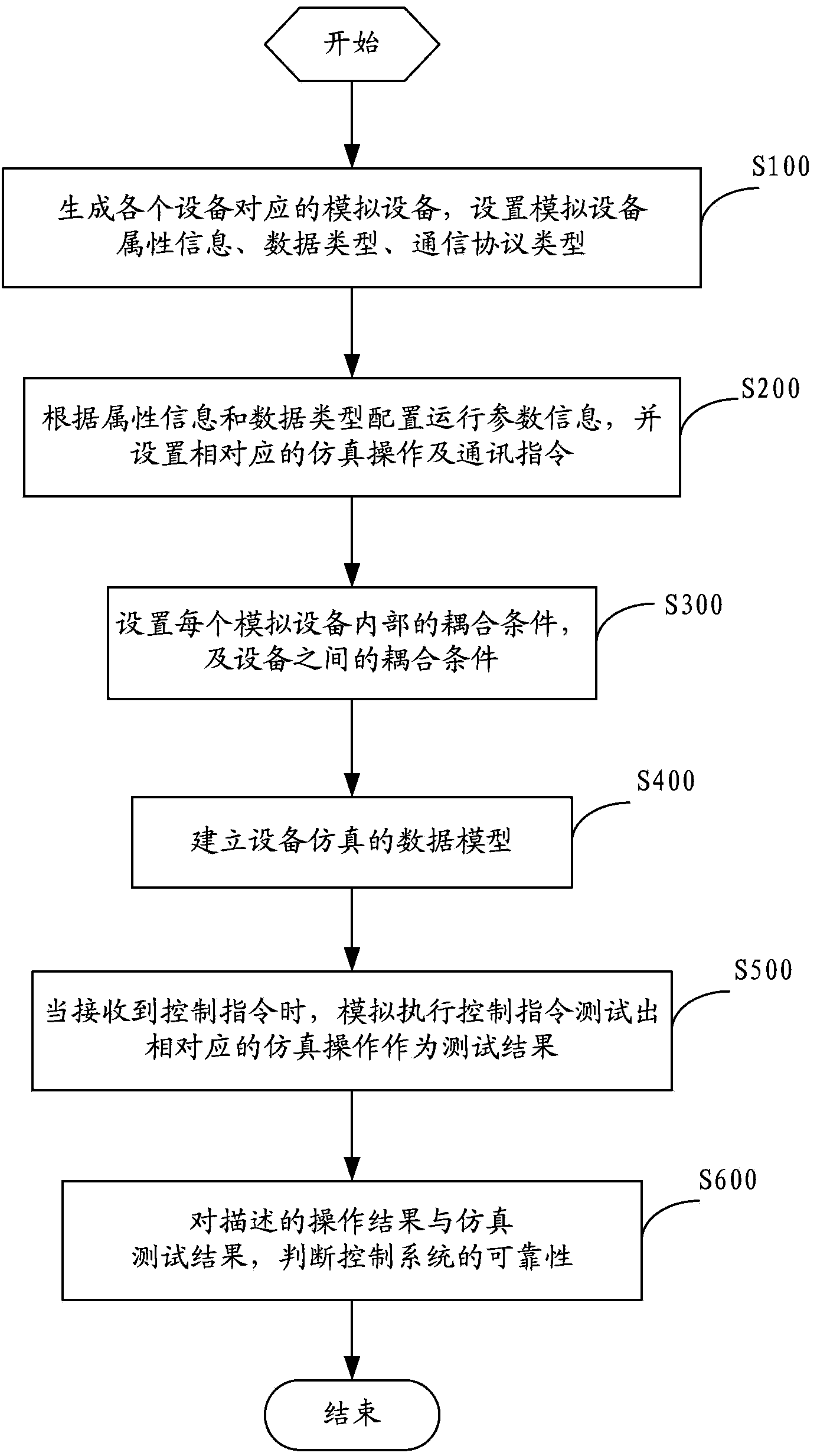
[0094] As an implementable form, the first embodiment provides the simulation test method of the control system in the semiconductor manufacturing process, which is applied to the simulation test of the vacuum control system controlling the pump, valve and pressure gauge in the vacuum system of the semiconductor manufacturing process, including the following The above steps:
[0095] Step S201. Generate each analog device corresponding to each semiconductor device (pump, valve, pressure gauge) in the vacuum system, and set the attribute information of each analog device, the data type of the attribute information of each analog device, and the vacuum machine where the vacuum control system is located. The type of communication protocol with each analog device;
[0096] First, the vacuum system includes pumps, valves and pressure gauges, which are turned on during normal operation. Specifically, taking the pressure gauge as an example, determine the attribute information of the...
PUM
 Abstract
Description
Claims
Application Information