Multiple frequency sputtering for enhancement in deposition rate and growth kinetics of dielectric materials

A sputtering target, sputtering deposition technology, applied in sputtering coating, metal material coating process, circuits, etc., can solve the problems of low thermal conductivity, particle generation, high capital expenditure requirements, etc.

Inactive Publication Date: 2014-05-21
APPLIED MATERIALS INC
View PDF13 Cites 2 Cited by
  • Summary
  • Abstract
  • Description
  • Claims
  • Application Information

AI Technical Summary

Problems solved by technology

Furthermore, these dielectric materials typically have low thermal conductivity, which limits sputtering processing at high frequencies to lower power density regimes to avoid problems such as thermal gradient-induced stresses in the sputtering target. problems that can lead to cracking and particle generation
Limitations to low power density conditions lead to relatively low deposition rates which in turn lead to high capital expenditure requirements for manufacturing systems with higher throughput

Method used


Image

  • Multiple frequency sputtering for enhancement in deposition rate and growth kinetics of dielectric materials
  • Multiple frequency sputtering for enhancement in deposition rate and growth kinetics of dielectric materials
  • Multiple frequency sputtering for enhancement in deposition rate and growth kinetics of dielectric materials

Examples


Embodiment Construction

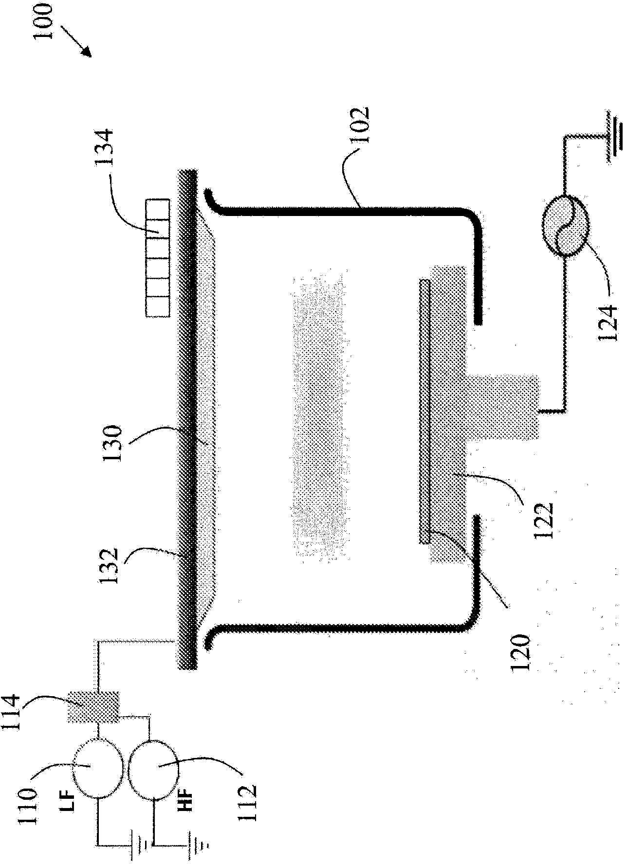
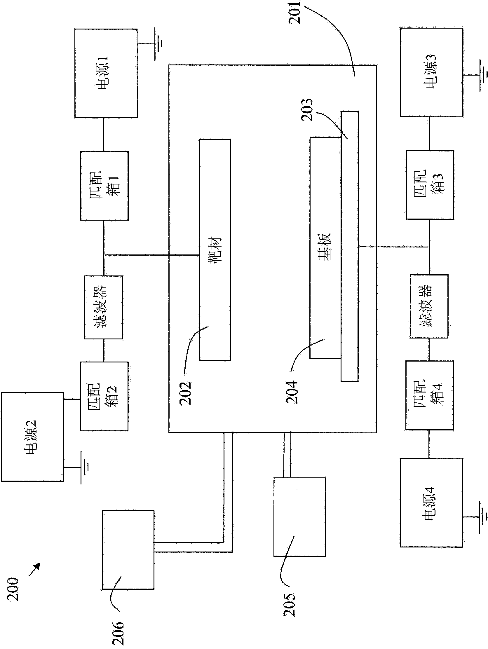
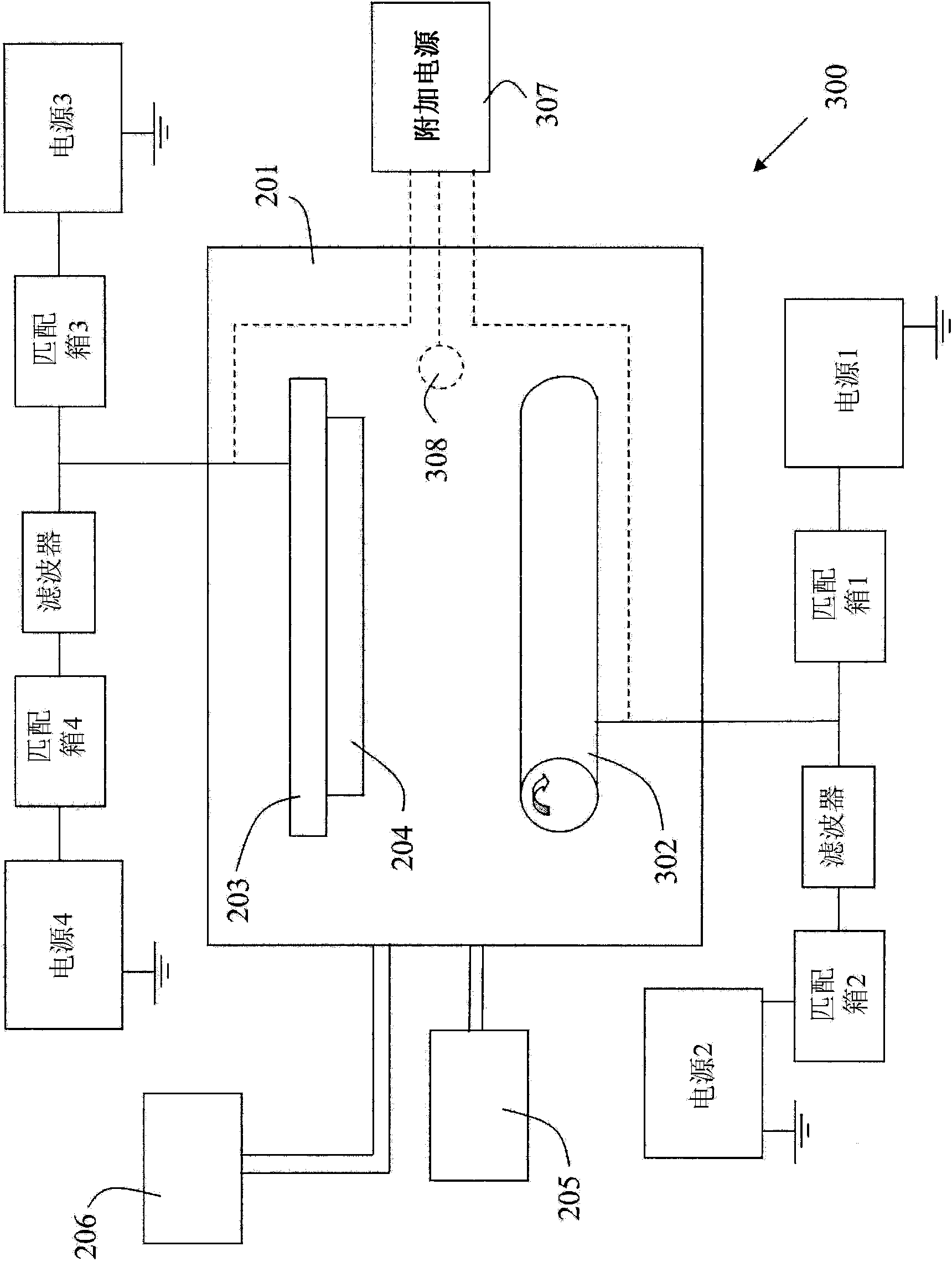
[0022] Embodiments of the present invention, provided as illustrative examples of the invention so as to enable those skilled in the art to practice the invention, will now be described in detail with reference to the accompanying drawings. Significantly, the figures and examples below are not meant to limit the scope of the invention to a single embodiment, but other embodiments are possible by interchanging some or all of the described or illustrated elements. Furthermore, in the case where certain elements of the present invention can be partially or completely implemented using known components, only those parts of the known components necessary for understanding the present invention will be described, and descriptions will be omitted. Detailed descriptions of other parts of known components are used so as not to obscure the invention. In this specification, an embodiment illustrating a single component should not be considered limiting; rather, the invention is intended ...


PUM


Abstract

A method of sputter depositing dielectric thin films may comprise: providing a substrate on a substrate pedestal in a process chamber, the substrate being positioned facing a sputter target; simultaneously applying a first RF frequency from a first power supply and a second RF frequency from a second power supply to the sputter target; and forming a plasma in the process chamber between the substrate and the sputter target, for sputtering the target. The first RF frequency is less than the second RF frequency, the first RF frequency is chosen to control the ion energy of the plasma and the second RF frequency is chosen to control the ion density of the plasma. The self-bias of surfaces within said process chamber may be selected; and this is enabled by connecting a blocking capacitor between the substrate pedestal and ground.

Description

[0001] Cross References to Related Applications [0002] This application claims the benefit of US Provisional Application No. 61 / 533,074, filed September 9, 2011, which is hereby incorporated by reference in its entirety. technical field [0003] Embodiments of the present invention relate generally to apparatus for deposition of dielectric thin films, and more particularly to sputtering apparatus for dielectric thin films that include a multi-frequency power supply. Background technique [0004] Usually such as Li 3 PO 4 Dielectric materials such as LiPON (Lithium Phosphorus Nitride Oxide) are used to form LiPON, mainly due to the extremely low conductivity of said dielectric materials, high frequency power (radio frequency, RF) is required to achieve dielectric targets for thin film deposition (PVD) sputtering. Furthermore, these dielectric materials generally have low thermal conductivity, which limits sputtering processing at high frequencies to lower power density...

Claims


Application Information

Patent Timeline
Patent Type & Authority Applications(China)
IPC IPC(8): H01L21/203H01L21/31
CPCC23C14/345C23C14/3471H01J37/32165H01J37/3405C23C14/00
Inventor 冲·蒋秉·圣·利奥·郭迈克尔·斯托厄尔卡尔·阿姆斯特朗
Owner APPLIED MATERIALS INC
Why Eureka
Try Eureka