Plasma process uniformity across a wafer by controlling RF phase between opposing electrodes

a plasma and opposing electrode technology, applied in the direction of coatings, electric discharge lamps, electric lighting sources, etc., can solve the problems of reducing the uniformity of the rf field, the wafer surface is not uniform, and the process is not uniform, so as to reduce the non-uniformity of the edge-high non-uniformity, increase the current flow, and reduce the current flow

Inactive Publication Date: 2008-07-31
APPLIED MATERIALS INC
View PDF11 Cites 39 Cited by
  • Summary
  • Abstract
  • Description
  • Claims
  • Application Information

AI Technical Summary

Benefits of technology

[0007]In an embodiment, said adjusting includes bringing said phase difference closer to an angle of 180 degrees in order to increase current flow between the two electrodes and decrease current flow to the edge ground return path so as to decrease an edge-high non-uniformity in plasma ion density distribution. In a different embodiment, said adjusting includes bringing said phase difference closer to an angle of zero degrees in order to decrease current flow between the two electrodes and increase current flow to the edge ground ret...

Problems solved by technology

One problem inherent in such a plasma source is that the ceiling electrode exhibits radial transmission line effects and loading due to the effective dielectric constant of the plasma.
Therefore, the RF field varies significantly across the surface of the ceiling electrode, giving rise to process non-uniformities at the wafer surface.
For a plasma with an effective dielectric constant greater than 1, the effective wavelength is reduced to less than the ceiling electrode diameter, worsening the non-uniformity of the RF field, making processing non-uniformities across the wafer surface worse.
For an etch process, this may produce a non-uniform edge low etch rate distribution across the wafer surface.
One problem with this approach is that a...

Method used


Image

  • Plasma process uniformity across a wafer by controlling RF phase between opposing electrodes
  • Plasma process uniformity across a wafer by controlling RF phase between opposing electrodes
  • Plasma process uniformity across a wafer by controlling RF phase between opposing electrodes

Examples


Embodiment Construction

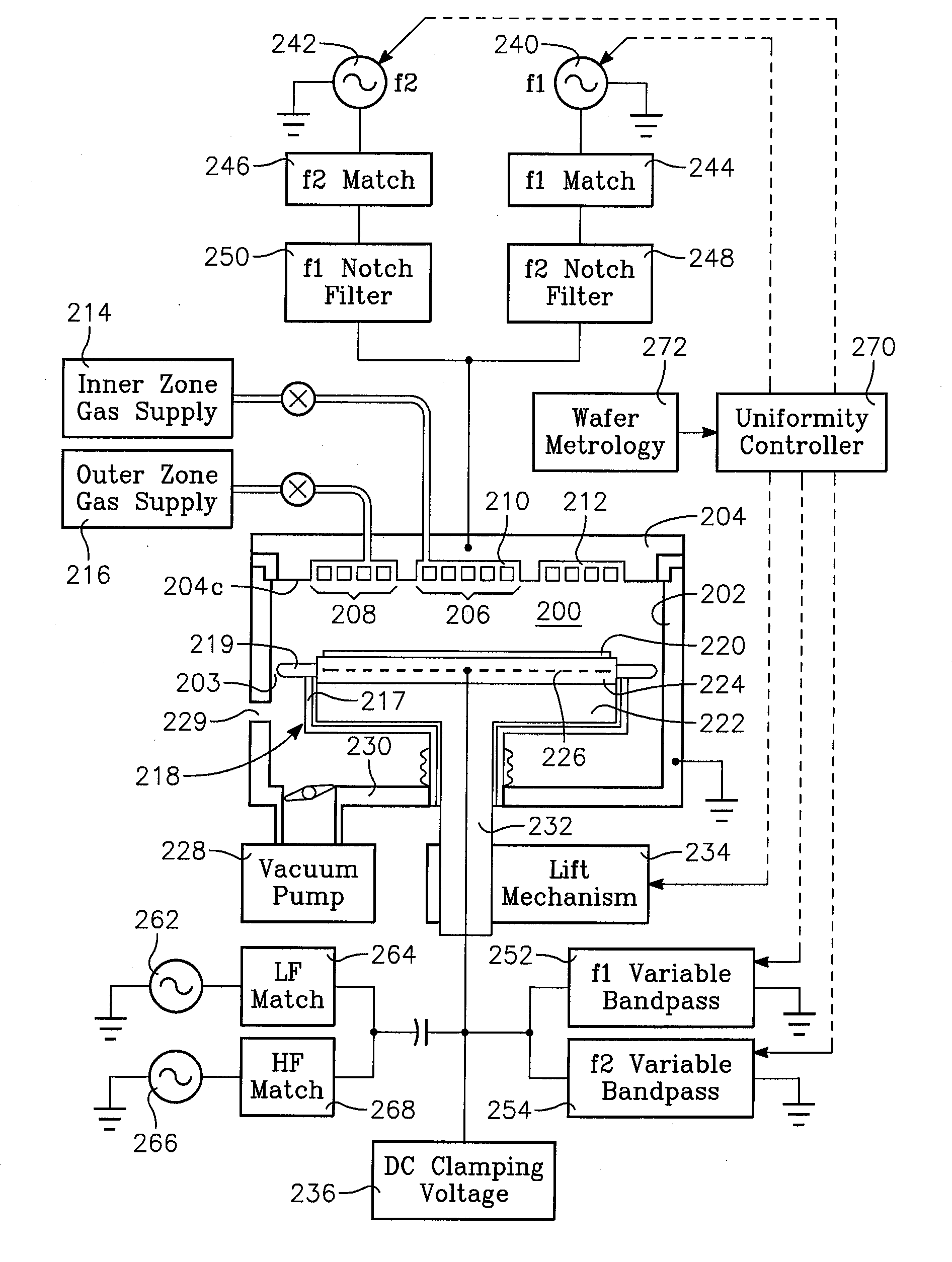
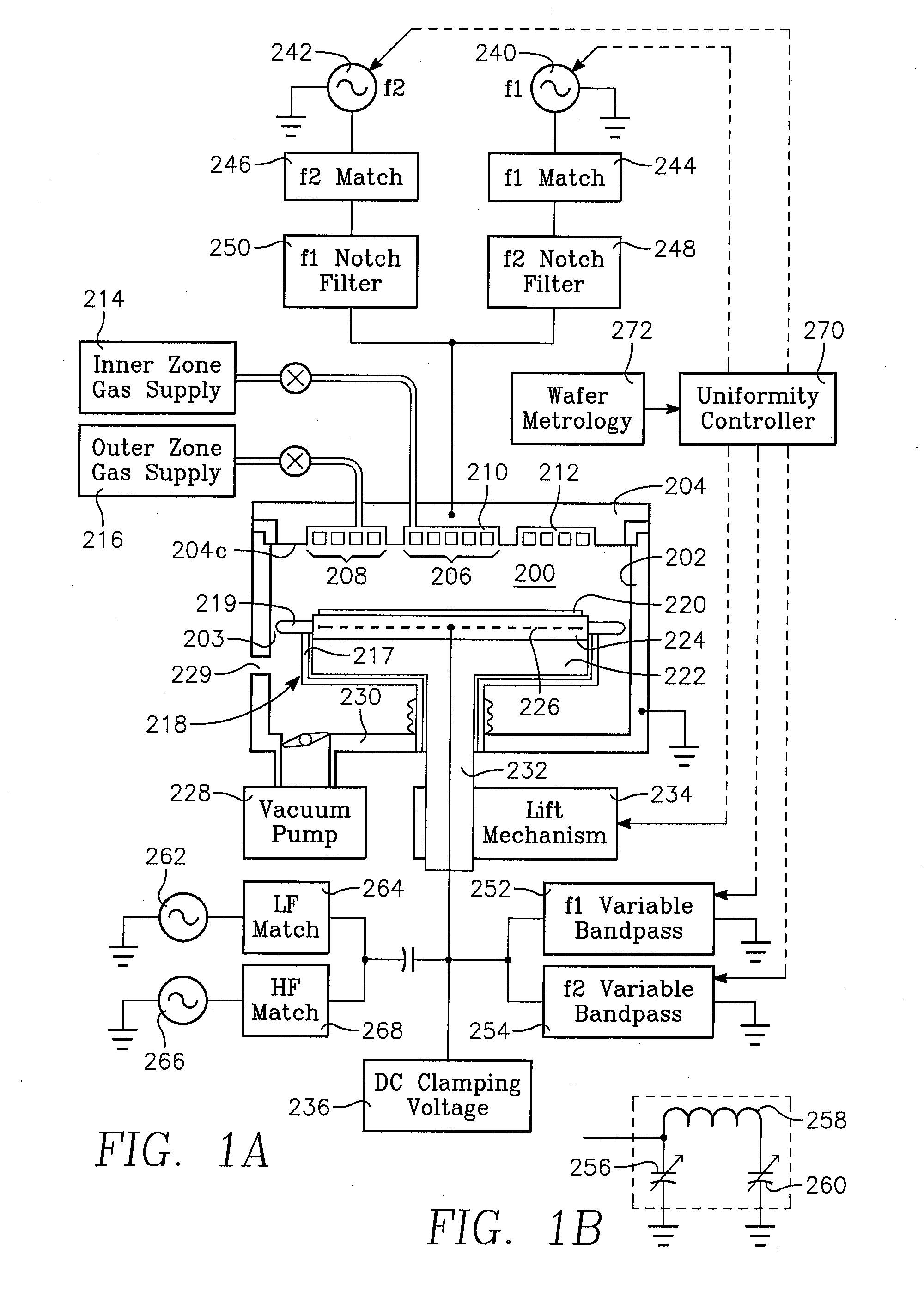
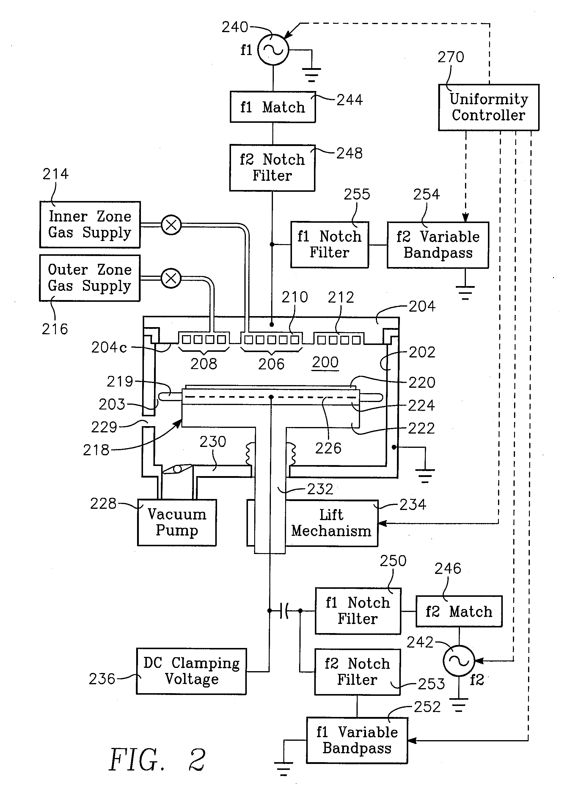
[0026]FIG. 1A is a simplified schematic diagram of a plasma reactor capable of controlling radial distribution of plasma ion density by apportioning capacitively coupled plasma source power among different source power frequencies. The reactor has a vacuum chamber 200 enclosed by a cylindrical side wall 202 and a disk-shaped ceiling 204. The ceiling 204 is both a conductive ceiling electrode as well as a gas distribution showerhead or plate, and will be referred to herein as the ceiling electrode 204. The ceiling electrode may optionally be covered with a conducting, semiconducting or insulating material. The ceiling electrode 204 includes inner and outer zones 206, 208 of gas injection orifices on its bottom surface 204c coupled to respective inner and outer internal gas manifolds 210, 212. Inner and outer zone process gas supplies 214, 216 furnish process gases to the inner and outer manifolds 210, 212. A wafer support pedestal 218 can support a workpiece such as a semiconductor w...


PUM

PropertyMeasurementUnit
Angleaaaaaaaaaa
Angleaaaaaaaaaa
Angleaaaaaaaaaa

Abstract

A method is provided for processing a workpiece in a plasma reactor chamber. The method includes coupling, to a plasma in the chamber, power of an RF frequency via a ceiling electrode and coupling, to the plasma, power of at least approximately the same RF frequency via a workpiece support electrode. The method also includes providing an edge ground return path. The method further includes adjusting the proportion between (a) current flow between said electrodes and (b) current flow to the edge ground return path from said electrodes, to control plasma ion density distribution uniformity over the workpiece.

Description

CROSS-REFERENCE TO RELATED APPLICATIONS[0001]This application claims the benefit of U.S. Provisional Application Ser. No. 60 / 898,632, filed Jan. 30, 2007.BACKGROUND[0002]Embodiments of the present invention concern a capacitively coupled plasma source for processing a workpiece such as a semiconductor wafer. A capacitively coupled plasma source comprises a ceiling electrode that is driven at a very high frequency (VHF) frequency over 110 MHz which can produce a high density plasma at a relatively low voltage. A capacitively coupled plasma source can further produce a low electrode potential for low electrode erosion, and permits the ion energy at the wafer surface to be limited to a low level if desired, while operating over a wide range of plasma density (very low to very high plasma ion density). One problem inherent in such a plasma source is that the ceiling electrode exhibits radial transmission line effects and loading due to the effective dielectric constant of the plasma. Fo...

Claims


Application Information

Patent Timeline
IPC IPC(8): H01J7/00
CPCC23C16/45574C23C16/5096H01J37/32091H01L21/6831H01J37/32174H01L21/67069H01J37/32165
Inventor COLLINS, KENNETH S.HANAWA, HIROJIRAMASWAMY, KARTIKBUCHBERGER, DOUGLAS A.RAUF, SHAHIDBERA, KALLOLWONG, LAWRENCEMERRY, WALTER R.MILLER, MATTHEW L.SHANNON, STEVEN C.NGUYEN, ANDREWCRUSE, JAMES P.CARDUCCI, JAMESDETRICK, TROY S.DESHMUKH, SUBHASHSUN, JENNIFER Y.
Owner APPLIED MATERIALS INC
Why Eureka
Try Eureka