Supercharge Your Innovation With Domain-Expert AI Agents!

Pattern forming method, electron beam-sensitive or extreme ultraviolet-sensitive composition, resist film, method for manufacturing electronic device using the same, and electronic device

A technology for extreme ultraviolet rays and electronic devices, applied in the fields of pattern formation, electron beam sensitive or extreme ultraviolet sensitive compositions, resist films, the use of which to manufacture electronic devices and electronic devices, capable of solving problems such as poor resolution of pattern outlines , to achieve the effect of high resolution, high sensitivity, high line width roughness

Inactive Publication Date: 2014-05-28
FUJIFILM CORP
View PDF33 Cites 0 Cited by
  • Summary
  • Abstract
  • Description
  • Claims
  • Application Information

AI Technical Summary

Problems solved by technology

[0004] In particular, in order to shorten the wafer processing time, improvement in sensitivity is very important, but when higher sensitivity is pursued, the pattern profile or the reso

Method used


Image

  • Pattern forming method, electron beam-sensitive or extreme ultraviolet-sensitive composition, resist film, method for manufacturing electronic device using the same, and electronic device
  • Pattern forming method, electron beam-sensitive or extreme ultraviolet-sensitive composition, resist film, method for manufacturing electronic device using the same, and electronic device
  • Pattern forming method, electron beam-sensitive or extreme ultraviolet-sensitive composition, resist film, method for manufacturing electronic device using the same, and electronic device

Examples


Embodiment

[0947]

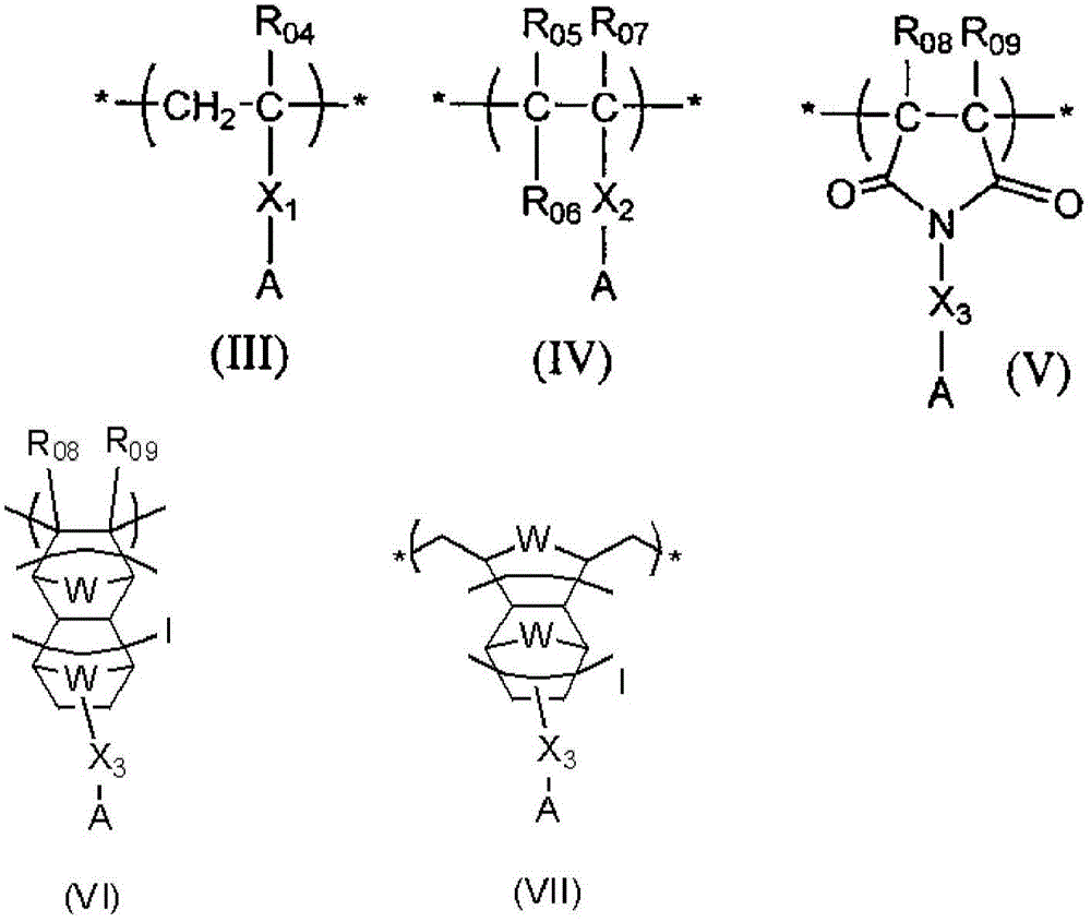
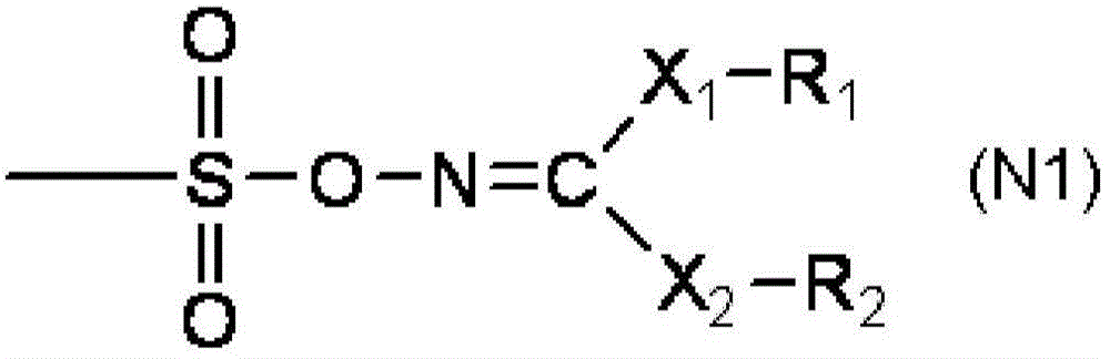
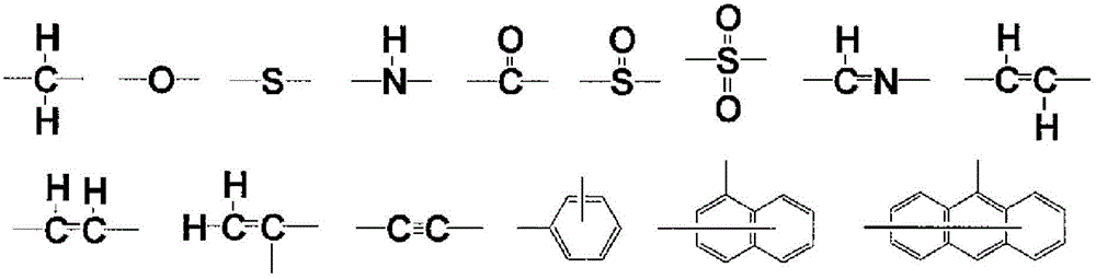
[0948] Resins (A-1) to (A-24), (RA-1) and (RA-2) shown below were synthesized as follows. The weight average molecular weight (Mw) and polydispersity (Mw / Mn) of each resin are shown below. Also, the composition ratio of each repeating unit of the resin is shown in molar ratio.

[0949]

[0950]

[0951]

[0952]

[0953]

Synthetic example 1

[0954] [Synthesis Example 1: Resin (A-1)]

[0955] In a nitrogen flow, 160 g of cyclohexanone was charged into a three-necked flask and heated at 80° C. (solvent 1). Subsequently, Monomer-A1 (13.58 g), Monomer-1 (23.11 g), Monomer-2 (12.48 g) and Monomer-3 (31.35 g) shown below were dissolved in cyclohexanone (297 g) to prepare a monomer solution. Further, a solution obtained by adding and dissolving a polymerization initiator V-601 (manufactured by Wako Pure Chemical Industries, Ltd.) at a rate of 6.4 mol% based on the monomer was added dropwise to Solvent 1 over 6 hours. After the dropwise addition was completed, the solution was further reacted at 80° C. for 2 hours. The reaction solution was cooled and then added dropwise to a mixed solvent of 3,000 g of heptane / 750 g of ethyl acetate, and the precipitated powder was collected by filtration and dried to obtain 62 g of Resin (A-1). The obtained resin (A-1) had a weight average molecular weight of 10,500, a polydispersity...

Embodiment 1 to 24 and comparative example 1 and 2

[0982] [Examples 1 to 24 and Comparative Examples 1 and 2 (electron beam (EB) exposure)]

[0983] (1) Preparation of Coating Solution of Electron Beam Sensitive or Extreme Ultraviolet Sensitive Resin Composition, and Coating

[0984] Coating solution compositions according to the formulations shown in the following table were microfiltered through a membrane filter having a pore size of 0.1 μm to obtain electron beam-sensitive or extreme ultraviolet-sensitive resin composition (resist composition) solutions.

[0985] This electron beam-sensitive or extreme ultraviolet-sensitive resin composition solution was coated on a 6-inch Si wafer previously treated with hexamethyldisilazane (HMDS) by using a spin coater Mark8 (manufactured by Tokyo Electron Ltd.) and dried on a hot plate at 100° C. for 60 seconds to obtain a resist film with a thickness of 50 nm.

[0986] (2) EB exposure and development

[0987] The resist film-coated wafer obtained in (1) above was subjected to patter...


PUM

PropertyMeasurementUnit
Thicknessaaaaaaaaaa

Abstract

There is provided a pattern forming method comprising (1) a step of forming a film by using an electron beam-sensitive or extreme ultraviolet-sensitive resin composition, (2) a step of exposing the film by using an electron beam or an extreme ultraviolet ray, and (3) a step of developing the exposed film by using an organic solvent-containing developer, wherein the electron beam-sensitive or extreme ultraviolet-sensitive resin composition contains (A) a resin containing (R) a repeating unit having a structural moiety capable of decomposing upon irradiation with an electron beam or an extreme ultraviolet ray to generate an acid, and (B) a solvent.

Description

technical field [0001] The present invention relates to a pattern forming method using a developer containing an organic solvent, an electron beam-sensitive or extreme ultraviolet-sensitive resin composition, and a resist film suitable for use in an ultramicrolithography process Such as the manufacture of VLSI or high-capacity microchips or other optical manufacturing processes, and the present invention also relates to a method of manufacturing an electronic device using the same, and an electronic device. More specifically, the present invention relates to a resist pattern forming method using a developer containing an organic solvent, an electron beam-sensitive or extreme ultraviolet-sensitive resin composition, and a resist film which can be suitably used for Semiconductor microprocessing using electron beams or EUV light (wavelength: close to 13 nm), and also relates to a manufacturing method of an electronic device using the same, and an electronic device. Background t...

Claims


Application Information

Patent Timeline
IPC IPC(8): G03F7/038G03F7/004G03F7/039G03F7/32H01L21/027
CPCG03F7/0388G03F7/405G03F7/32G03F7/0045G03F7/2041G03F7/038G03F7/325G03F7/0046G03F7/039G03F7/004G03F7/11G03F7/0392G03F7/0397
Inventor 泷泽裕雄岩户薰椿英明
Owner FUJIFILM CORP
Features
  • R&D
  • Intellectual Property
  • Life Sciences
  • Materials
  • Tech Scout
  • Unparalleled Data Quality
  • Higher Quality Content
  • 60% Fewer Hallucinations
Learn More