Method for achieving high-speed data transmission and universal interface chip

A technology of high-speed data transmission and general interface, applied in transmission systems, electrical digital data processing, climate sustainability, etc., can solve problems such as difficult to guarantee QoS, increase chip complexity and power consumption level, and achieve reduction of complexity and Effects on power consumption levels, guaranteed speed and quality

Active Publication Date: 2014-06-04
SANECHIPS TECH CO LTD
View PDF6 Cites 5 Cited by
  • Summary
  • Abstract
  • Description
  • Claims
  • Application Information

AI Technical Summary

Problems solved by technology

High-speed interfaces often have higher logic complexity and protocol standards, which increase the complexity and power consumption of the chip while obtaining higher transmission bandwidth
The low-speed transmission interface has simple logic design characteristics, but because of its simple protocol, it is difficult to guarantee the QoS (Quality of Service) of its transmission in actual application.

Method used


Image

  • Method for achieving high-speed data transmission and universal interface chip
  • Method for achieving high-speed data transmission and universal interface chip
  • Method for achieving high-speed data transmission and universal interface chip

Examples


Embodiment Construction

[0022] It should be understood that the specific embodiments described here are only used to explain the present invention, not to limit the present invention.

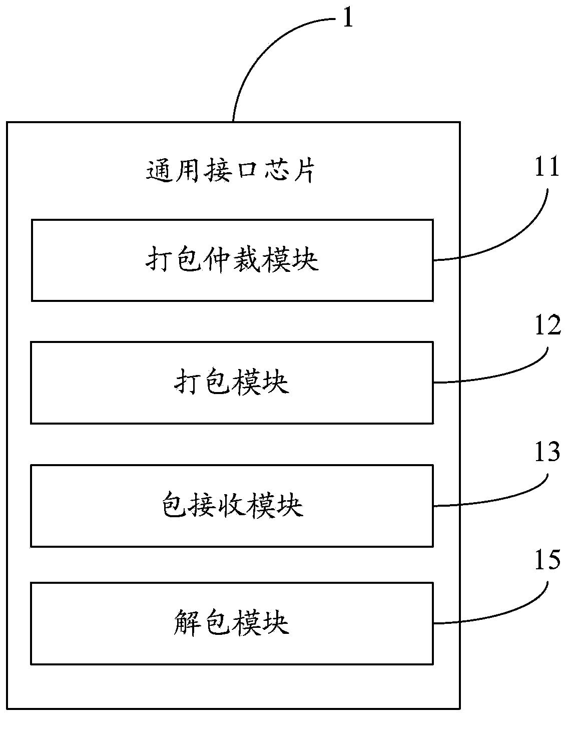
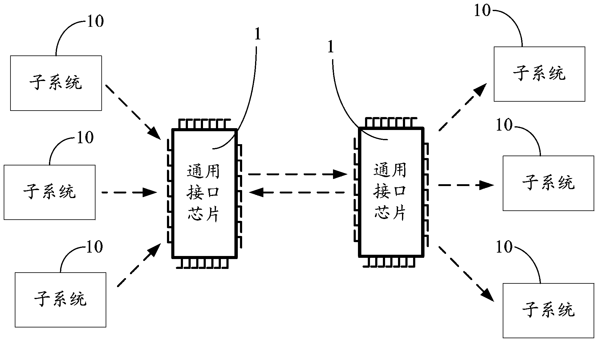
[0023] Such as figure 1 Shown is a system architecture diagram of a preferred embodiment of the general interface chip of the present invention. The universal interface chip 1 is used for data exchange and communication transmission, for example figure 2 As shown, the general interface chip 1 at the sending end sends the data of at least one subsystem 10 (take 3 as an example in the figure) that maintains communication interconnection with it to at least one subsystem that maintains communication interconnection with the general interface chip 1 at the receiving end. System 10 (three in the figure as an example). The number of connection pins (pins) of the physical layer of the universal interface chip 1 is variable.

[0024] The general interface chip 1 includes a packet arbitration module 11 , a packet module 12...


PUM


Abstract

The invention provides a method for achieving high-speed data transmission. According to the method, the preset bit wide is utilized to package a data packet to be transmitted again, checking codes are added into the data packet, system resources are released at once with regard to correct response information, the data packet is automatically retransmitted with regard to wrong response information, therefore, complexity and power consumption of a chip are reduced, and data exchange speed and quality are ensured. The invention further provides a universal interface chip for achieving high-speed data transmission.

Description

technical field [0001] The invention relates to an interface chip data transmission technology, in particular to a method for realizing high-speed data transmission and a general interface chip. Background technique [0002] With the rapid development of contemporary application-specific integrated circuits, the application of integrated circuits (chips) has penetrated into various fields. In the design of electronic circuit systems, the simple system solution consisting of a single chip has been replaced by a multi-chipset solution. The relationship between chips in a single board is closer, and interconnection and mutual access between chips cannot be avoided. At the same time, with the rapid increase in the number of services and the increase in business complexity, the problem of chip interconnection and mutual access has gradually become the bottleneck of the performance of the system, the whole machine and the single board. Therefore, we urgently need a more general, h...

Claims


Application Information

Patent Timeline
IPC IPC(8): G06F13/38G06F13/42H04L47/2475H04L47/6275
CPCY02B60/1228G06F13/00G06F13/4282Y02D10/00H04L47/2475H04L47/6275H04L47/628H04L49/552
Inventor 陈续陈德炜冯立国徐洪波
Owner SANECHIPS TECH CO LTD
Why Eureka
Try Eureka