Semiconductor device and manufacturing method thereof

A manufacturing method and semiconductor technology, applied in the fields of semiconductor devices, semiconductor/solid-state device manufacturing, electrical components, etc., can solve the problems of dielectric constant shift, threshold voltage shift, affecting the performance of semiconductor devices, etc., to improve performance, prevent The effect of oxidative invasion

Active Publication Date: 2017-08-25
SEMICON MFG INT (SHANGHAI) CORP
View PDF1 Cites 0 Cited by
  • Summary
  • Abstract
  • Description
  • Claims
  • Application Information

AI Technical Summary

Problems solved by technology

[0009] However, the dielectric constant of the gate dielectric layer 20 of the above-mentioned semiconductor device is prone to shift (shift), and correspondingly, the threshold voltage will also shift, which ultimately affects the performance of the semiconductor device

Method used


Image

  • Semiconductor device and manufacturing method thereof
  • Semiconductor device and manufacturing method thereof
  • Semiconductor device and manufacturing method thereof

Examples


Embodiment Construction

[0027] In order to make the above objects, features and advantages of the present invention more comprehensible, specific implementations of the present invention will be described in detail below in conjunction with the accompanying drawings.

[0028] In the following description, many specific details are set forth in order to fully understand the present invention, but the present invention can also be implemented in other ways than those described here, so the present invention is not limited by the specific embodiments disclosed below.

[0029] As mentioned in the background art, the dielectric constant of the gate dielectric layer in the prior art is prone to shift, thereby degrading the performance of the semiconductor device.

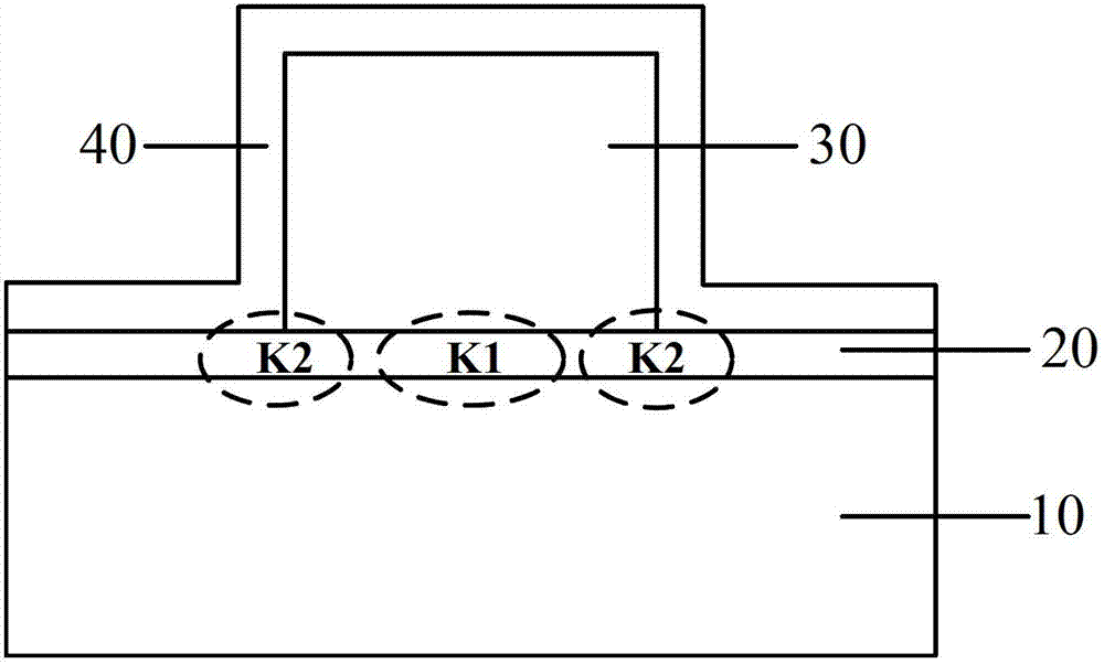
[0030] The inventor found through research: continue to refer to figure 1 As shown, in order to increase the dielectric constant of the gate dielectric layer 20 to K1, nitrogen atoms are doped into the gate dielectric layer 20 of silicon dioxide...


PUM


Abstract

Provided are a semiconductor device and a manufacturing method of the semiconductor device. The semiconductor device comprises a semiconductor substrate, a gate dielectric layer arranged on the semiconductor substrate, a grid electrode arranged on the gate dielectric layer and an oxidation layer at least arranged on the side wall of the grid electrode, the gate dielectric layer is made of oxynitride, and the oxidation layer is made of silicon oxynitride. The manufacturing method of the semiconductor device comprises the steps that the semiconductor substrate is provided; the gate dielectric layer made of oxynitride materials is formed on the semiconductor substrate; a polysilicon gate is formed on the gate dielectric layer; the oxidation layer made of silicon oxynitride materials is at least formed on the side wall of the polysilicon gate. The dielectric constant of the gate dielectric layer can be prevented from deviating, and the performance of the semiconductor device is improved at last.

Description

technical field [0001] The invention relates to the technical field of semiconductor manufacturing, in particular to a semiconductor device and a manufacturing method thereof. Background technique [0002] The main device of integrated circuits, especially ultra-large-scale integrated circuits, is metal-oxide-semiconductor field effect transistors (MOS transistors). The key performance index of MOS transistors is the drive current. The magnitude of the drive current depends on the gate capacitance, and the gate capacitance and The gate surface area is directly proportional to the thickness of the gate dielectric layer, and is proportional to the dielectric constant of the gate dielectric layer. The thickness of the gate dielectric layer should not be too small, otherwise impurities such as boron ions doped in the gate will diffuse from the gate into the semiconductor substrate or be fixed in the gate dielectric layer, thereby affecting the threshold voltage of the device. W...

Claims


Application Information

Patent Timeline
Patent Type & Authority Patents(China)
IPC IPC(8): H01L29/423H01L21/28H01L21/316
CPCH01L21/28247H01L21/28255H01L21/28264H01L21/285H01L29/518
Inventor 禹国宾
Owner SEMICON MFG INT (SHANGHAI) CORP
Why Eureka
Try Eureka