Fabrication method of fiber alignment pedestal array

A technology for optical fiber alignment and manufacturing methods, applied in the direction of optical waveguide and light guide, can solve the problems of high cost, optical signal power loss, low efficiency, etc., and achieve the effect of high output and stable process

Active Publication Date: 2016-04-13
SHANGHAI HUAHONG GRACE SEMICON MFG CORP
View PDF4 Cites 0 Cited by
  • Summary
  • Abstract
  • Description
  • Claims
  • Application Information

AI Technical Summary

Problems solved by technology

[0003] At present, the most commonly used method in the industry is to use laser melting glass to make fiber through-hole bases. The laser melting method has the disadvantages of rough manufacturing process, low alignment accuracy, high cost and low efficiency. Poor alignment of optical fibers leads to loss of optical signal power. Serious problem, urgently need a high-precision, low-cost and high-yield manufacturing process to replace it

Method used


Image

  • Fabrication method of fiber alignment pedestal array
  • Fabrication method of fiber alignment pedestal array
  • Fabrication method of fiber alignment pedestal array

Examples


Embodiment Construction

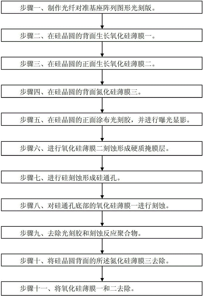
[0030] Such as figure 1 Shown is the flow chart of the method of the embodiment of the present invention; Figure 2A to Figure 2I Shown is a device structure diagram in each step of the method of the embodiment of the present invention. The manufacturing method of the optical fiber alignment base array in the embodiment of the present invention includes the following steps:

[0031] Step 1. Draw an array pattern of the fiber alignment base on the photolithographic plate, and the array pattern of the fiber alignment base defines the size and array of the holes of the fiber alignment base. The fiber alignment base array pattern includes a circular hole array pattern formed according to fiber size and fiber array arrangement, and a marking hole pattern for distinguishing the front and back of the fiber alignment base.

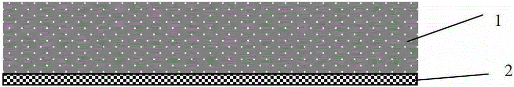
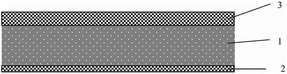
[0032] Step two, such as Figure 2A As shown, a silicon oxide film-2 is grown on the back surface of the silicon wafer 1, and the thickness of the silicon wafe...


PUM

PropertyMeasurementUnit
thicknessaaaaaaaaaa
thicknessaaaaaaaaaa
thicknessaaaaaaaaaa

Abstract

The invention discloses a method for manufacturing an optical fiber alignment substrate array. The method includes the steps of manufacturing a photolithography plate, growing a first silicon oxide film on the back face of a silicon wafer, growing a second silicon oxide film on the front face of the silicon wafer, growing a third silicon nitride film on the back face of the silicon wafer, coating the front face of the silicon wafer with photoresist, carrying out exposure development, etching the second silicon oxide film to form a hard mask layer, carrying out silicon etching to form silicon through holes, etching the positions, at the bottoms of the silicon through holes, of the first silicon oxide film, removing the photoresist and etched reaction polymer, removing the third silicon nitride film on the back face of the silicon wafer, removing the first silicon oxide film and the second silicon oxide film, and forming the optical fiber alignment substrate array. According to the method, the optical fiber alignment substrate array which is high in accuracy and small in size can be formed, the process is stable, the yield is high, faults when the silicon wafer is scanned by an infrared scanner in the production process can be eliminated, the method can be accordingly suitable for large-scale automation production, the use rate of production equipment can be accordingly improved, and the production efficiency can be accordingly improved.

Description

technical field [0001] The invention relates to a manufacturing process method of a semiconductor integrated circuit, in particular to a manufacturing method of an optical fiber alignment base array. Background technique [0002] At present, the application of optical communication devices is becoming more and more extensive, and fiber-to-the-home projects have also begun to be gradually implemented in economically developed areas. Multiple optical fiber channels are required for optical signal processing in an optical system, and long and thin optical fibers need to be fixed on a large number of optical fiber alignment bases (OFAs) to ensure that the quality of the fixed optical fibers meets system requirements. Therefore, high alignment accuracy and stable process are the basic requirements for low optical signal power loss. [0003] At present, the most commonly used method in the industry is to use laser melting glass to make fiber through-hole bases. The laser melting ...

Claims


Application Information

Patent Timeline
Patent Type & Authority Patents(China)
IPC IPC(8): G02B6/13
Inventor 陈瑜袁苑罗啸吴智勇
Owner SHANGHAI HUAHONG GRACE SEMICON MFG CORP
Why Eureka
Try Eureka