AI technical title is built by Patsnap AI team. It summarizes the technical point description of the patent document.
A Hall sensor and sensor technology, which is applied in the direction of magnetic sensor arrays, instruments, and electric power measurement by using electromagnetic effect devices, can solve the problems of limiting the accuracy of Hall sensors, reduce residual bias voltage, improve accuracy, The effect of reducing the electric field
Active Publication Date: 2014-06-18
AMS AG
View PDF6 Cites 11 Cited by
Summary
Abstract
Description
Claims
Application Information
AI Technical Summary
This helps you quickly interpret patents by identifying the three key elements:
Problems solved by technology
Method used
Benefits of technology
Problems solved by technology
However, relative to the sensitivity of the Hall sensor, if the described method is used, there is still a residual bias voltage greater than the voltage caused by the earth's magnetic field
The residual bias voltage thus limits the accuracy of the Hall sensor
Method used
Image
Click on the blue label to locate the original text in one second.
Reading with bidirectional positioning of images and text.
Examples
Embodiment Construction
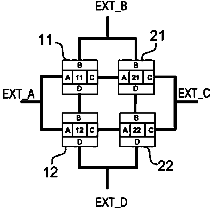
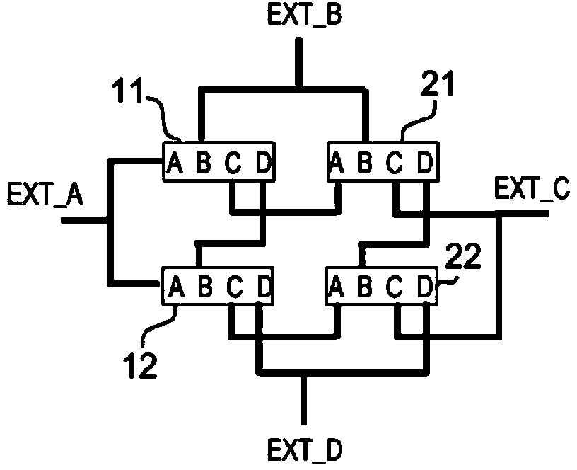
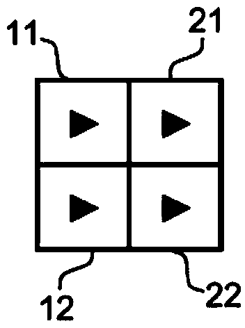
[0084] FIG. 1 shows different embodiments of a Hall sensor with several Hall sensor elements 11 , 12 , 21 , 22 which are interconnected and in this way together form a larger Hall sensor. . Figure 1A An embodiment with a lateral Hall sensor element is shown, while Figure 1B A vertical Hall sensor element is used in the exist Figure 1A with Figure 1B In the two embodiments illustrated in the Hall sensor elements 11, 12, 21, 22 respectively comprise four element terminals or element terminals A, B, C, D, some of which are connected to adjacent Hall sensor element, and some of the element terminals are connected to external terminals or sensor terminals EXT_A, EXT_B, EXT_C, EXT_D. The circuit is implemented similarly in both embodiments, so that the following description of the circuit can be applied to Figure 1A with Figure 1B .
[0085] In the Hall sensor, the element terminals A of the Hall sensor elements 11 , 12 are commonly connected to the sensor terminal EXT_...
PUM
Abstract
A Hall sensor has at least three Hall sensor elements (1, 2,..., 94) which each have at least three element connections (A, B, C, D, E, F, G, H) and are connected in a circuit grid having a structure which is more than one-dimensional, and at least three sensor connections (EXT_A, EXT_B, EXT_C, EXT_D) for making contact with the Hall sensor. In this case, each sensor connection (EXT_A, EXT_B, EXT_C, EXT_D) is connected to at least one of the Hall sensor elements (1, 2,..., 94) at one of the element connections (A, B, C, D, E, F, G, H) thereof.
Description
technical field [0001] The invention relates to a Hall sensor with several Hall sensor elements arranged on a semiconductor body. Background technique [0002] The Hall effect, named after American physicist Edwin Herbert Hall (1855-1938), occurs when a magnetic field perpendicular to the current is present. In this case, the magnetic field produces a potential difference called Hall voltage in a direction extending perpendicular to the direction of the magnetic field and perpendicular to the direction of the current flow. The measurement of the Hall voltage enables the determination of the magnitudes of the components of the magnetic field. [0003] Hall sensors for measuring Hall voltages may be implemented in the form of semiconductor devices. The evaluation circuit can also be integrated into the semiconductor component and can be produced, for example, during a CMOS process. If the plane of the active region in which the operating current flows and in which the Hall ...
Claims
Application Information
Patent Timeline
Application Date:The date an application was filed.
Publication Date:The date a patent or application was officially published.
First Publication Date:The earliest publication date of a patent with the same application number.
Issue Date:Publication date of the patent grant document.
PCT Entry Date:The Entry date of PCT National Phase.
Estimated Expiry Date:The statutory expiry date of a patent right according to the Patent Law, and it is the longest term of protection that the patent right can achieve without the termination of the patent right due to other reasons(Term extension factor has been taken into account ).
Invalid Date:Actual expiry date is based on effective date or publication date of legal transaction data of invalid patent.

