Touch display device and manufacturing method thereof

A technology of touch display and production method, which is applied in the fields of optics, instruments, electrical digital data processing, etc., to achieve the effect of improving quality

Inactive Publication Date: 2014-06-25
BOE TECH GRP CO LTD +1
View PDF7 Cites 16 Cited by
  • Summary
  • Abstract
  • Description
  • Claims
  • Application Information

AI Technical Summary

Problems solved by technology

[0006] The technical problem to be solved by the present invention is how to eliminate the adverse effects of the above-mentioned coupling capacitance on touch detection, so as to improve the quality of the touch display device.

Method used


Image

  • Touch display device and manufacturing method thereof
  • Touch display device and manufacturing method thereof
  • Touch display device and manufacturing method thereof

Examples


Embodiment 1

[0043] The touch display device of this embodiment is based on the on-cell technology in the embedded touch technology,

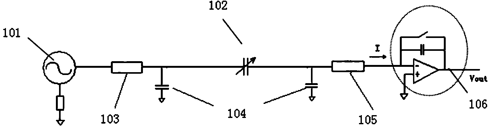
[0044]Specifically, the touch display device provided in this embodiment includes a first substrate and a second substrate oppositely arranged, a liquid crystal layer between the first substrate and the second substrate, and a separation layer formed on the first substrate. separated receiving electrodes, on the first substrate, a separated first transparent electrode is arranged below the receiving electrodes in the projection direction of the first substrate along the display electrodes on the second substrate , the first transparent electrode is separated from the receiving electrode by an insulating layer, and the first transparent electrode is used for connecting to a fixed potential. Wherein, the formation of the liquid crystal layer may be by dripping liquid crystals between the two substrates after the first substrate and the second substrate are bo...

Embodiment 2

[0048] This embodiment is based on the embedded in-cell technology, the emitter electrode is located on the side of the array substrate, and the receiving electrode is located on the side of the color filter substrate. Here, the first substrate is the color filter substrate, and the second substrate is the array substrate as an example. This embodiment will be described.

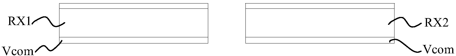
[0049] Based on the above situation, this embodiment proposes a touch display device with a new structure, referring to Figure 4 As shown, it includes: a first substrate 1 and a second substrate 6 oppositely arranged, a liquid crystal layer 5 formed between the first substrate 1 and the second substrate 6, and a liquid crystal layer formed on the first substrate 1 Separated receiving electrodes RX, the color filter layer 4 is formed on the first substrate 1 , and an array structure is formed on the second substrate 6 , such as gate, source-drain, common electrode and other structures.

[0050] The array su...

Embodiment 3

[0055] This embodiment is based on the embedded in-cell touch technology of the ADS display mode, and a touch display device in which the emitting electrodes and the receiving electrodes are both on the side of the color filter substrate.

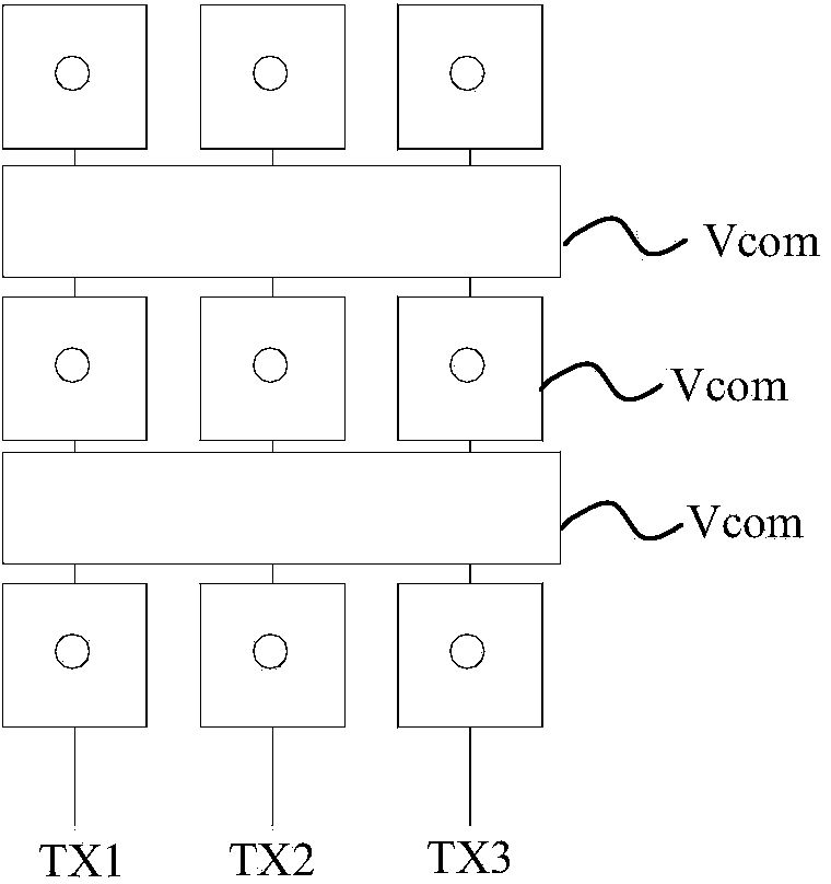
[0056] The structure of the touch display device in this embodiment is as follows: Figure 7 As shown, it includes: a first substrate 1 and a second substrate 6 oppositely arranged, a liquid crystal layer 5 formed between the first substrate 1 and the second substrate 6, and a liquid crystal layer formed on the first substrate 1 The receiving electrodes RX and the transmitting electrodes TX are arranged at intervals, a color filter layer is formed on the first substrate 1, and an array structure is formed on the second substrate 6, such as Figure 7 The display electrode 7 shown in (for example, including gate layer, source and drain, pixel electrode and common electrode, etc.); in order to eliminate the coupling capacitance between the rec...


PUM


Abstract

The invention discloses a touch display device and a manufacturing method of the touch display device. The touch display device comprises a first substrate, a second substrate, a liquid crystal layer, separated receiving electrodes and first separated transparent electrodes, the first substrate and the second substrate are oppositely arranged, the liquid crystal layer is arranged between the first substrate and the second substrate, the separated receiving electrodes are formed on the first substrate, the first separated transparent electrodes are formed below the receiving electrodes, in the projection direction of the first substrate, on the first substrate and along a display electrode on the second substrate, the first transparent electrodes and the receiving electrodes are separated by insulation layers, and the first transparent electrodes are connected to fixed potentials. When the receiving electrodes and emission electrodes are arranged on the same layer, coupling capacitors between the receiving electrodes and the electrodes on an array substrate and between emission layers and the thelectrodes on the array substrate are shielded. When the emission electrodes are arranged on the array substrate side, coupling capacitors between the receiving electrodes and a common electrode of the array substrate side and coupling capacitors formed between the emission electrodes and the receiving electrodes through the liquid crystal layer are shielded. When liquid crystals deflect, detection signals are not influenced basically, noise caused by frame switching is shielded, and the quality of the touch display device is improved obviously.

Description

technical field [0001] The present invention relates to the field of touch technology, in particular to a touch display device and a manufacturing method thereof. Background technique [0002] As an input medium, a touch screen provides users with better convenience than a keyboard and a mouse. According to different implementation principles, touch screens can be classified into resistive, capacitive, surface acoustic wave, infrared, etc., and resistive and capacitive touch screen technologies are widely used at present. [0003] Mutual capacitive touch screen, with its high sensitivity and advantages of multi-touch, is becoming more and more popular. The basic principle of mutual capacitive touch screen is: apply voltage on the drive line side, and detect signal changes on the detection line side , the driving line determines the X-direction coordinates, and the detection line determines the Y-direction coordinates. During detection, the X-direction driving lines are sca...

Claims


Application Information

Patent Timeline
Patent Type & Authority Applications(China)
IPC IPC(8): G06F3/041G02F1/1333G02F1/1343
CPCG06F3/0412G06F3/0443G06F3/0445G06F3/0446G06F2203/04112G06F2203/04103
Inventor 丁小梁董学王海生刘英明任涛
Owner BOE TECH GRP CO LTD
Why Eureka
Try Eureka