Printed Wiring Board, Printed Circuit Board, And Method For Manufacturing Printed Circuit Board
一种印刷布线板、印刷电路板的技术,应用在印刷电路制造、印刷电路、印刷电路等方向,能够解决不具有电子部件、没有表现出散热效果等问题
- Summary
- Abstract
- Description
- Claims
- Application Information
AI Technical Summary
Problems solved by technology
Method used
Image

Examples
no. 1 example
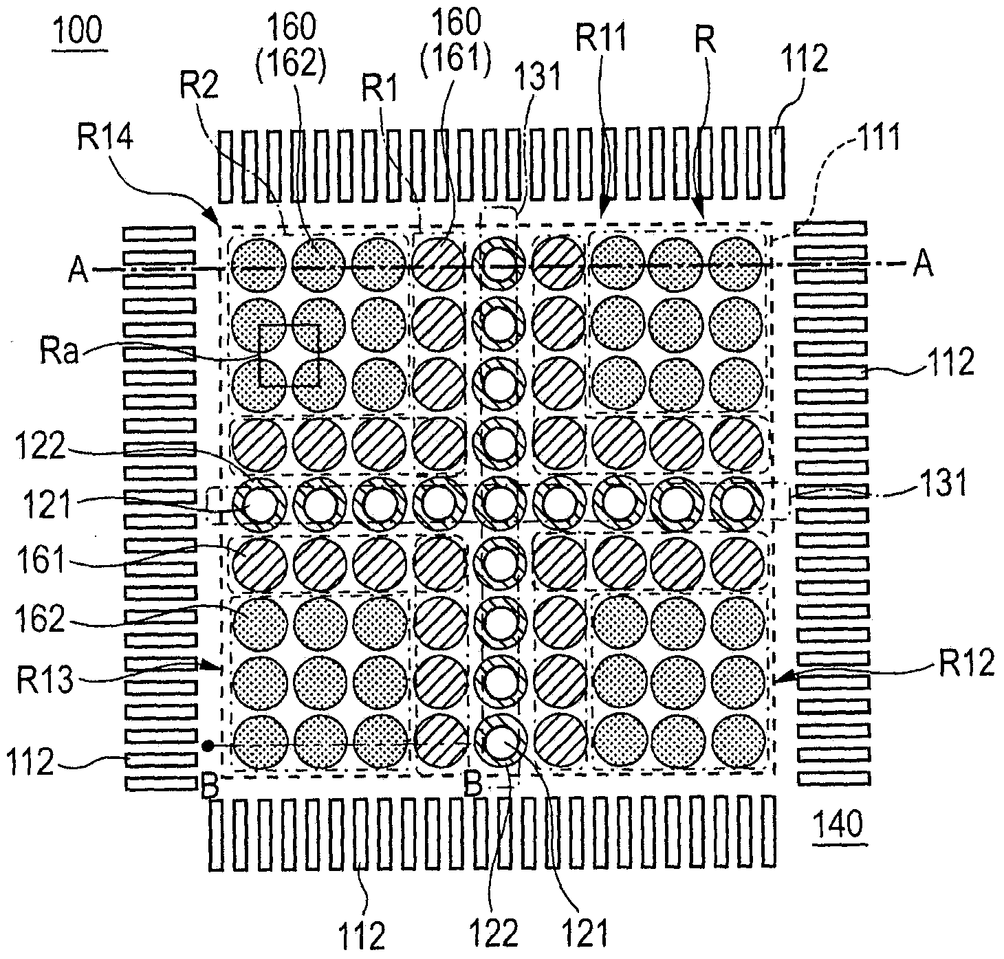
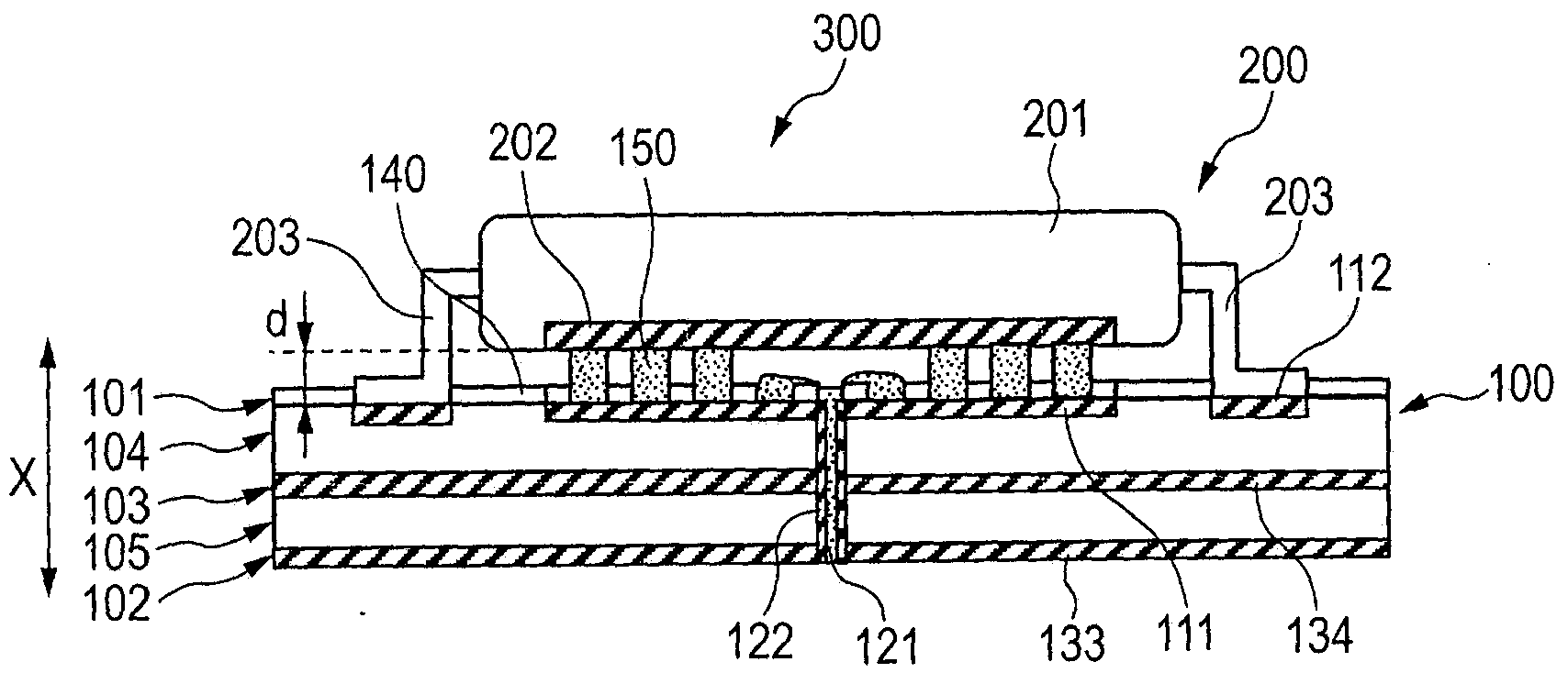
[0026] Figure 1A and 1B is an explanatory view showing a schematic configuration of the printed circuit board according to the first embodiment of the present invention. Figure 1A is a plan view showing a part of the printed wiring board on which electronic components are mounted; Figure 1B is along the Figure 1A A cross-sectional view of the printed circuit board taken on line A-A. The printed circuit board 300 includes the semiconductor package 200 serving as an electronic component and the printed wiring board 100 . The semiconductor package 200 is mounted on the printed wiring board 100 .
[0027] The semiconductor package 200 is a QFP (Quad Flat Pack) type semiconductor package. The semiconductor package 200 includes a quadrangular (rectangular parallelepiped) package body 201 , a quadrangular heat sink 202 provided on the rear surface (bottom surface) of the package body 201 , and a plurality of leads (electrodes) 203 protruding from the package body 201 . The pac...
no. 2 example
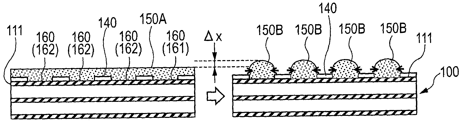
[0065] exist Figure 1A and 1B In the illustrated first embodiment, the pad 161 is formed in the first region R1 directly adjacent to the through hole 121, the pad 162 is formed in the second region R2, and the pad 161 exists in the second region R2 and the between the through holes 121 . However, regarding the second region R2, the pad 161 need not exist between the second region R2 and the through hole 121, but the gap between the through hole 121 and the pad 162 may be a value equal to or greater than a certain value.
[0066] A printed circuit board according to a second embodiment of the present invention will be described below. Figure 4 is a plan view showing a printed wiring board 100H according to the second embodiment. Incidentally, in the second embodiment, the description about the electronic component mounted on the printed wiring board and the solder joint portion connecting the heat sink of the electronic component and the heat transfer pattern of the printed...
no. 3 example
[0079] Next, a printed circuit board according to a third embodiment of the present invention will be described below. Image 6 is a plan view showing a printed wiring board 100A according to a third embodiment of the present invention. Incidentally, in the third embodiment, the description about the electronic component mounted on the printed wiring board and the solder joint portion connecting the heat sink of the electronic component and the heat transfer pattern of the printed wiring board to each other is omitted. In addition, in the printed wiring board, configurations similar to those in the above-described first embodiment are designated by the same reference numerals, and the description will be omitted.
[0080] Further, in the third embodiment, the electronic component is a QFP type semiconductor package having a configuration similar to that of the semiconductor package 200 in the above-described first embodiment, and is mounted on the printed wiring board of the s...
PUM
 Abstract
Description
Claims
Application Information
 - Generate Ideas
- Intellectual Property
- Life Sciences
- Materials
- Tech Scout
- Unparalleled Data Quality
- Higher Quality Content
- 60% Fewer Hallucinations
Browse by: Latest US Patents, China's latest patents, Technical Efficacy Thesaurus, Application Domain, Technology Topic, Popular Technical Reports.
© 2025 PatSnap. All rights reserved.Legal|Privacy policy|Modern Slavery Act Transparency Statement|Sitemap|About US| Contact US: help@patsnap.com