Placement method of lithography alignment mark

A photolithographic alignment and marking technology, applied in the field of integrated circuit manufacturing, to achieve the effect of placing alignment marks

Inactive Publication Date: 2014-07-02
SHANGHAI HUAHONG GRACE SEMICON MFG CORP
View PDF5 Cites 4 Cited by
  • Summary
  • Abstract
  • Description
  • Claims
  • Application Information

AI Technical Summary

Problems solved by technology

[0005] The technical problem to be solved by the present invention is to provide a method for placing photolithographic alignment marks, which can solve the problem of placing photolithographic alignment marks when the cutting line size is less than 50 microns

Method used


Image

  • Placement method of lithography alignment mark
  • Placement method of lithography alignment mark
  • Placement method of lithography alignment mark

Examples


Embodiment Construction

[0016] In order to have a more specific understanding of the technical content, characteristics and effects of the present invention, now in conjunction with the illustrated embodiment, the details are as follows:

[0017] The specific method of placing the photolithographic alignment mark in this embodiment is as follows:

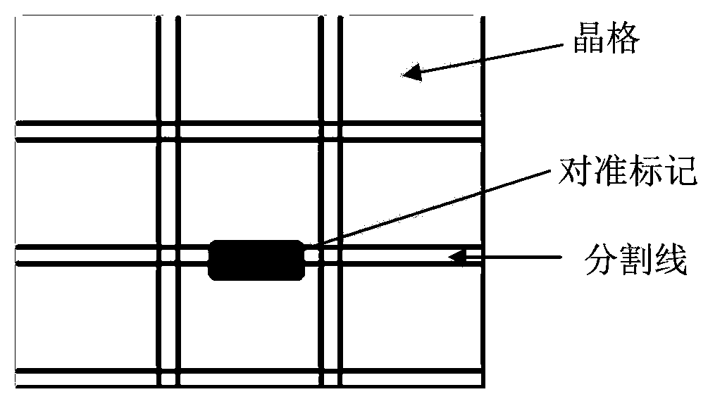
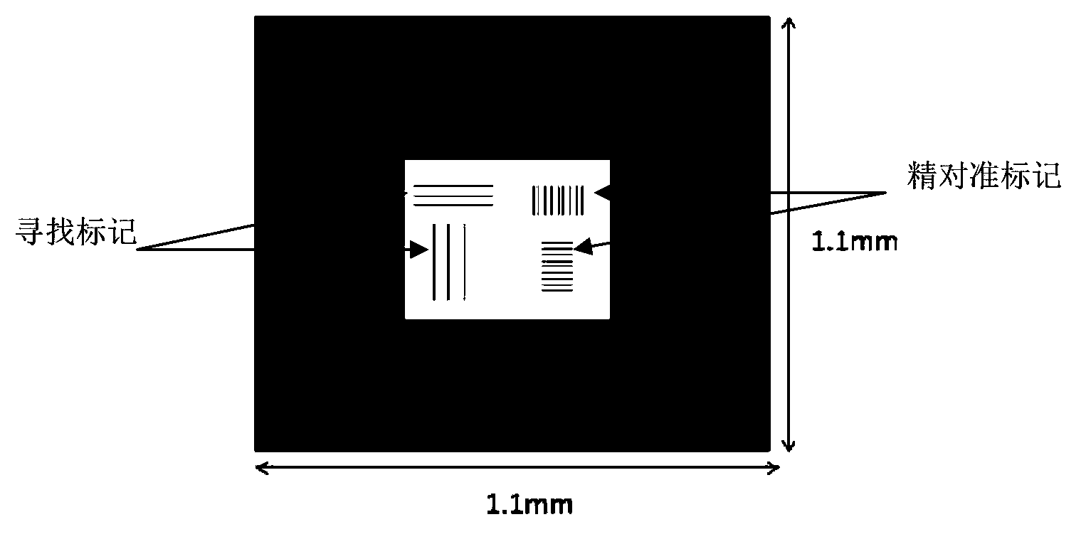
[0018] Step 1, first, integrate the search mark (search mark) and EGA mark (fine alignment mark) required for lithography in a space of 0.5mm×0.5mm on the mask to make an integrated pattern, plus 0.3mm chromium protection area, and make a photolithography plate together with the main pattern of the current layer, such as figure 2 shown. Calculate the coordinates of each photolithographic alignment mark relative to the center of the integrated pattern. For example, the coordinates of the search mark relative to the center of the integrated graphics are (Xs, Ys).

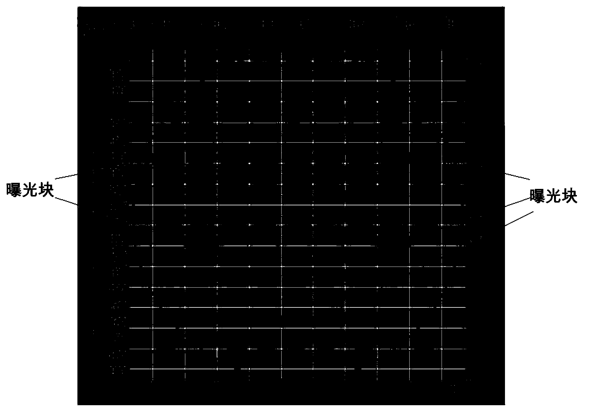
[0019] Step 2, according to the size of the lattice, select five special areas on the wafe...


PUM


Abstract

The invention discloses a placement method of lithography alignment marks. The method comprises the following steps: 1) integrating all lithography alignment marks in a graphic area of a mask to form a lithography mask with the main pattern of the current layer; 2) calculating a coordinate of each lithography alignment mark relative to the center of the integrated graphic; 3) according to the size of the lattice, selecting a plurality of special areas in the wafer for placing the integrated graphic; 4) imaging the integrated graphic on the lithography mask to the special areas in the wafer by using an exposure machine; and 5) for lithography of a next layer, translating the integrated graphic on the upper layer for alignment. According to the method provided by the invention, the lithography alignment marks are integrated and placed in the plurality of special areas in the wafer, and shot translation is used to realize lithography alignment; and the method is not limited by the size of a cutting line, hence solving the problem of placement of alignment mark after diminishing of the size of the cutting line.

Description

technical field [0001] The invention relates to the field of integrated circuit manufacturing, in particular to a method for placing photolithography alignment marks for cutting lines below 50 microns. Background technique [0002] For products with small crystal lattice (die), the smaller scribe line can greatly improve the utilization rate of silicon wafers. For example, for an 8-inch silicon wafer, for a lattice of 1.5mm×1.5mm, when the cutting line width is 80μm, the chip occupies 89.3% of the silicon wafer area; when the cutting line width is 20μm, the chip occupies 97.3% of the silicon wafer area. The smaller the cutting line, the higher the utilization rate of the silicon wafer. [0003] However, the current lithography exposure machines that use cutting line marks for alignment, such as Nikon lithography exposure machines, gradually reduce the size of the cutting line, CD (Critical Dimension, key dimension) and OVL (Overlay, registration accuracy) Although the meas...

Claims


Application Information

Patent Timeline
Patent Type & Authority Applications(China)
IPC IPC(8): G03F9/00G03F7/20
Inventor 丁刘胜
Owner SHANGHAI HUAHONG GRACE SEMICON MFG CORP
Why Eureka
Try Eureka