Fingerprint detection circuit and fingerprint detection device

A fingerprint detection and circuit technology, applied in the acquisition/organization of fingerprints/palmprints, character and pattern recognition, instruments, etc., can solve the problems of slow fingerprint detection, unstable circuit loop, poor circuit stability, etc. The effect of detection speed, high reliability and low circuit cost

Inactive Publication Date: 2014-07-02
SHENZHEN GOODIX TECH CO LTD
View PDF3 Cites 28 Cited by
  • Summary
  • Abstract
  • Description
  • Claims
  • Application Information

AI Technical Summary

Problems solved by technology

[0003] However, this technical solution has the following defects: firstly, because the capacitance of the capacitor component is very small, the resistor 30 is required to be very large in order to obtain an appropriate cut-off frequency, and it will consume a lot of cost to integrate it on the chip; secondly, when detecting a single fingerprint pixel It needs to go through multiple "comparator detection -> input signal adjustment" cycles to determine the final DC level. The higher the detection accuracy, the longer the detection cycle is required, resulting in the incompatibility of the two important indicators of detection speed and detection accuracy. ; Finally, the signal generation source 40 of this patent and the analog-to-digital converter constitute a closed-loop loop, so that the circuit has the risk of loop instability
[0004] To sum up, the existing fingerprint detection circuit has high circuit cost, poor circuit stability, and slow fingerprint detection speed.

Method used


Image

  • Fingerprint detection circuit and fingerprint detection device
  • Fingerprint detection circuit and fingerprint detection device
  • Fingerprint detection circuit and fingerprint detection device

Examples


Embodiment Construction

[0025] It should be understood that the specific embodiments described here are only used to explain the present invention, not to limit the present invention.

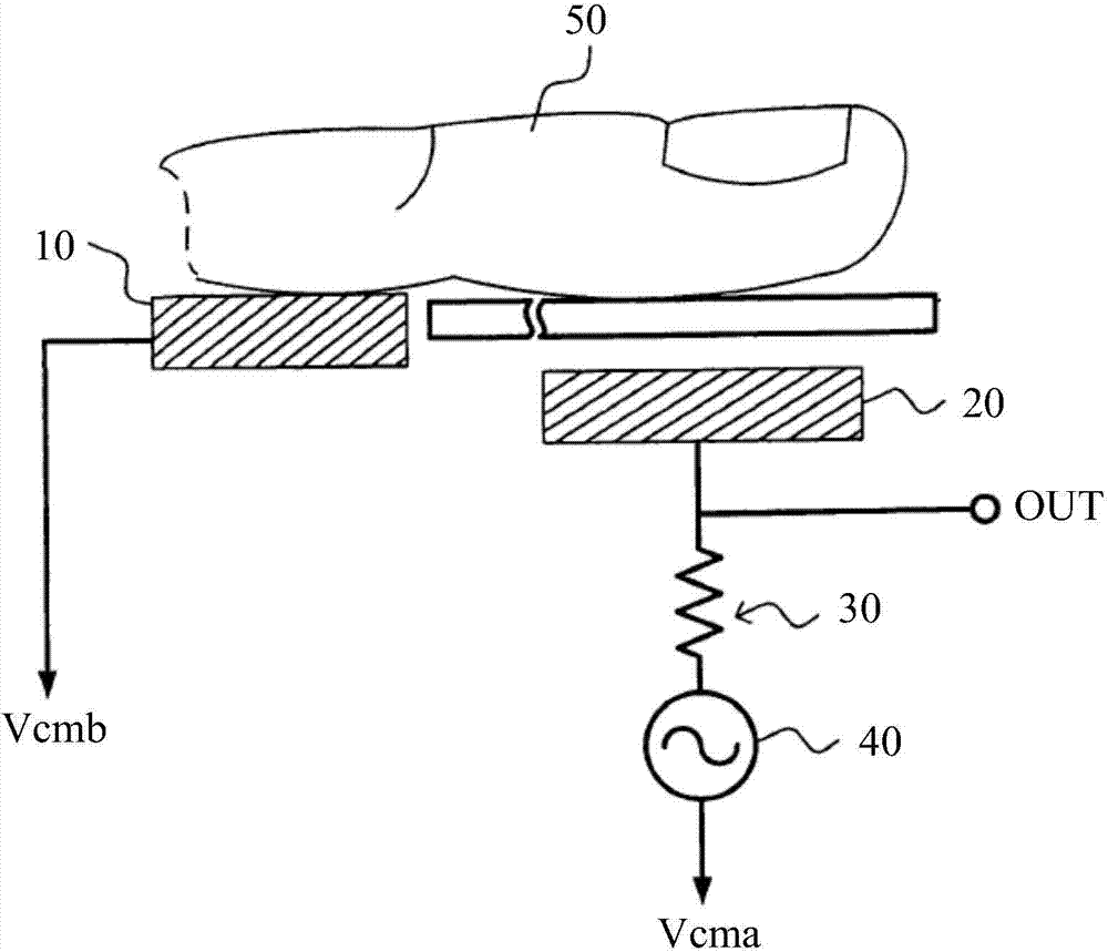
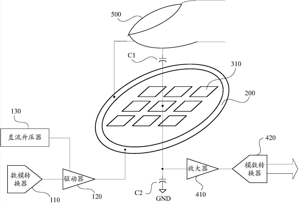
[0026] The fingerprint detection circuit of the present invention is a capacitive pressure-dividing fingerprint detection circuit, which utilizes the difference in size of the first capacitance C1 (or induction capacitance) corresponding to the "peak" and "valley" contained in the fingerprint, so it is excited by the same AC signal. Under the principle that the amplitude of the output signal is also different, the image information of the "peak" and "valley" is converted into a corresponding electrical signal.

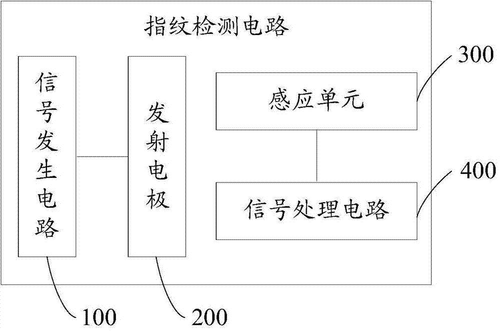
[0027] see figure 1 , figure 2 , an embodiment of the fingerprint detection circuit of the present invention is proposed, the fingerprint detection circuit includes a signal generating circuit 100, a transmitting electrode 200, a sensing unit 300 and a signal processing circuit 400, wherein the signal genera...


PUM


Abstract

The invention discloses a fingerprint detection circuit and a fingerprint detection device. The fingerprint detection circuit comprises a signal generation circuit, an emitting electrode, an induction unit and a signal processing circuit, wherein the signal generation circuit is used for generating an alternating-current signal, the emitting electrode is used for transmitting the alternating-current signal to fingers, the induction unit is used for collecting fingerprint information of the fingers, the signal processing circuit is used for processing the fingerprint information, and the signal generation circuit is electrically connected with the emitting electrode and the induction unit respectively. In this way, the alternating-current signal with a certain amplitude is coupled to the fingers by the emitting electrode so that a voltage division signal can be formed by the alternating-current signal through a first capacitor formed between the fingers and the induction unit and a second capacitor formed between the induction unit and the ground, output data including fingerprint information are generated after the voltage division signal is processed through the signal processing circuit, and finally fingerprint detection can be completed. Because an open-loop structure is adopted in the whole circuit and any feedback circuit is not adopted, the circuit is low in cost, high in reliability and high in fingerprint detection speed.

Description

technical field [0001] The invention relates to the technical field of fingerprint detection, in particular to a fingerprint detection circuit and a fingerprint detection device with the fingerprint detection circuit. Background technique [0002] In the fingerprint detection device, the fingerprint detection circuit is the core module used to convert the image information of the "peak" and "valley" contained in the fingerprint into an electrical signal. Chinese patent 200710129193.0 discloses a fingerprint detection circuit, which includes an external electrode 10, a detection unit 20, a resistor 30 and a signal generation source 40, the external electrode 10 and the signal generation source 40 are respectively coupled to reference levels Vcmb and Vcma, and the detection unit 20 is coupled to a signal generating source 40 through a resistor 30 , and the detection circuit further includes an output terminal OUT coupled between the detection unit 20 and the resistor 30 , and ...

Claims


Application Information

Patent Timeline
Patent Type & Authority Applications(China)
IPC IPC(8): G06K9/00
CPCG06V40/1306
Inventor 詹昶
Owner SHENZHEN GOODIX TECH CO LTD
Why Eureka
Try Eureka