
Pump capacitor multiplexing circuit, charge pump, flash memory and pump capacitor multiplexing method

A flash memory and multiplexing circuit technology, applied in the direction of conversion equipment without intermediate conversion to AC, can solve the problems of unfavorable flash memory layout area design optimization, large space for pump capacitors, etc., to achieve layout area optimization and design optimization , The effect of facilitating the promotion and application

Active Publication Date: 2017-01-25
INST OF MICROELECTRONICS CHINESE ACAD OF SCI
View PDF8 Cites 0 Cited by
  • Summary
  • Abstract
  • Description
  • Claims
  • Application Information

AI Technical Summary

Problems solved by technology

[0004] However, since the pump capacitor (comprising the first pump capacitor group 102 and the second pump capacitor group 202) and the filter capacitor occupy a large space in the flash memory, it is not conducive to the design of the layout area of ​​the flash memory. optimization

Method used


Image

  • Pump capacitor multiplexing circuit, charge pump, flash memory and pump capacitor multiplexing method
  • Pump capacitor multiplexing circuit, charge pump, flash memory and pump capacitor multiplexing method
  • Pump capacitor multiplexing circuit, charge pump, flash memory and pump capacitor multiplexing method

Examples


Embodiment 1

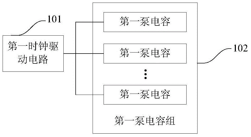
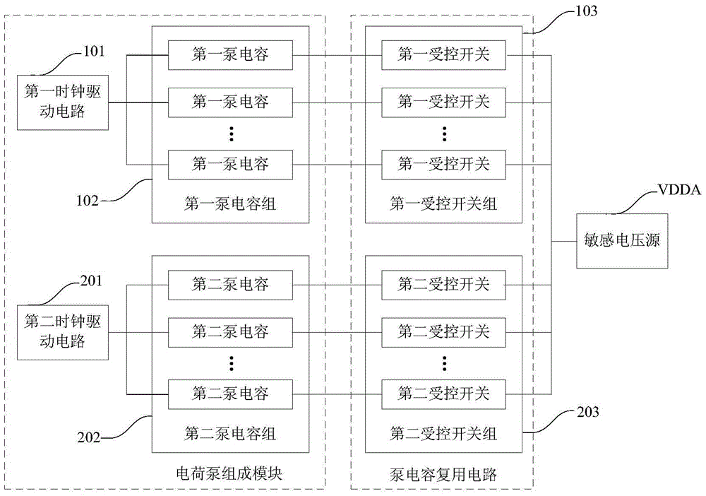
[0052] see figure 2 , Embodiment 1 of the present invention discloses a pump capacitor multiplexing circuit, which is applied to a flash memory to realize design optimization of the layout area of ​​the flash memory; specifically, the pump capacitor multiplexing circuit includes:

[0053] The first controlled switch group 103, the second controlled switch group 203 and the control circuit (not shown in the figure);

[0054] Wherein, the first controlled switch group 103 includes first controlled switches whose number is equal to the number of the first pump capacitors in the first pump capacitor combination 102; each of the first controlled switches is located in one of the first The connection point between the pump capacitor and the sensitive voltage source VDDA;

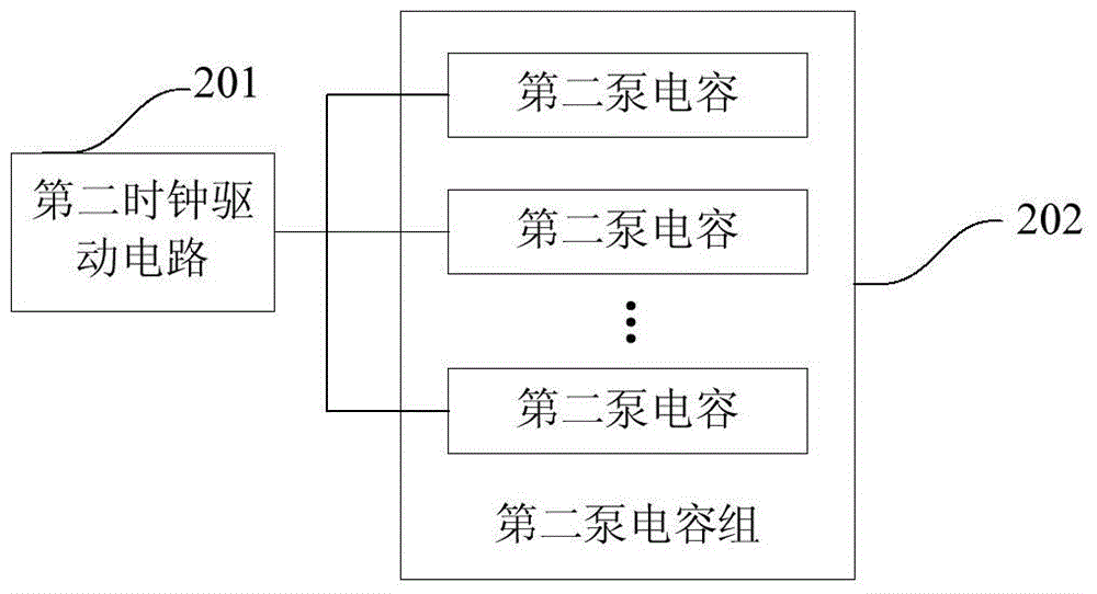
[0055] The second controlled switch group 203 includes second controlled switches equal to the number of the second pump capacitors in the second pump capacitor group 202; each of the second controlled switches ...

Embodiment 2

[0066] Based on Embodiment 1, Embodiment 2 of the present invention discloses yet another pump capacitor multiplexing circuit, which is applied to a flash memory to realize design optimization of the layout area of ​​the flash memory. The pump capacitor multiplexing circuit includes:

[0067] a first controlled switch group, a second controlled switch group and a control circuit;

[0068] Among them, the first controlled switch group and the second controlled switch group described in the second embodiment are compared with the first controlled switch group 103 and the second controlled switch group 203 described in the first embodiment in terms of circuit connection relationship and structural composition. There is no difference in

[0069] The control circuit described in the second embodiment is used for

[0070] Acquiring the operating mode information of the flash memory, the first clock signal output by the first clock drive circuit, and the second clock signal output b...

Embodiment 3

[0076] Based on Embodiment 2, Embodiment 3 of the present invention discloses yet another pump capacitor multiplexing circuit, which is applied to a flash memory to realize design optimization of the layout area of ​​the flash memory. See image 3 , the pump capacitor multiplexing circuit includes:

[0077] The first controlled switch group 103, the second controlled switch group 203 and the control circuit 300;

[0078] Wherein, each of the first controlled switches in the first controlled switch group 103 and each of the second controlled switches in the second controlled switch group 203 can use MOS transistors; the advantage is that the MOS transistors ( Also known as power MOSEEF) has many advantages such as high switching speed, high operating frequency, and good thermal stability;

[0079] There are various types and structures of the MOS tubes, and the most widely used NMOS tubes can be preferred in the third embodiment; the NMOS tubes have the working characteristics...


PUM


Abstract

The embodiment of the invention discloses a pump capacitor multiplex circuit applied to a flash memory. The circuit comprises a first controlled switch group, a second controlled switch group and a control circuit. Each controlled switch is located on the connection point of one first pump capacitor and a sensitive voltage source, and each second controlled switch is located on the connection point of one second pump capacitor and the sensitive voltage source. When the flash memory works in a read mode, the control circuit is used for controlling the first controlled switch group to be switched on if a first clock drive circuit outputs a low-level clock signal, and controlling the second controlled switch group to be switched on if a second clock drive circuit outputs a low-level clock signal, otherwise, the control circuit controls both the first controlled switch group and the second controlled switch group to be switched off to achieve design optimization of the layout area of the flash memory. Besides, the invention further discloses a pump capacitor multiplex method, a charge pump and the flash memory.

Description

technical field [0001] The invention relates to the technical field of flash memory development, more specifically, to a pump capacitor multiplexing circuit, a charge pump, a flash memory and a pump capacitor multiplexing method. Background technique [0002] The basic composition circuit of the flash memory includes: a charge pump, a power supply sensitive circuit (such as a sense amplifier), a sensitive voltage source, and a filter capacitor connected to the output of the sensitive voltage source; wherein the charge pump includes several charge Pump components. [0003] Specifically, see Figure 1a-1b , said any charge pump component module includes a first clock drive circuit 101, a second clock drive circuit 201, a first pump capacitor bank 102 and a second pump capacitor bank 202; wherein, the first clock drive circuit 101 and the second clock drive circuit The clock signal output by the drive circuit 201 is inverted, the first pump capacitor group 102 includes several...

Claims


Application Information

Patent Timeline
Patent Type & Authority Patents(China)
IPC IPC(8): H02M3/07
Inventor 龙爽陈岚陈巍巍杨诗洋
Owner INST OF MICROELECTRONICS CHINESE ACAD OF SCI
Learn More