Printed circuit board blind hole manufacturing method and structure

A technology for printed circuit boards and manufacturing methods, which is applied in the directions of printed circuit components, electrical connection printed components, and electrical connection formation of printed components, etc., which can solve the problems of high investment requirements, chemical corrosion modification residues, and poor surface smoothness of copper layers, etc. problem, achieve the effect of reducing signal transmission loss, improving surface smoothness, and avoiding drug residue

Active Publication Date: 2014-07-09
NAT CENT FOR ADVANCED PACKAGING
View PDF4 Cites 2 Cited by
  • Summary
  • Abstract
  • Description
  • Claims
  • Application Information

AI Technical Summary

Problems solved by technology

[0003] The conventional blind hole production process is to drill holes in the insulating material, and carry out hole metallization to connect the upper and lower layers of lines; since the hole metallization is directly carried out on the hole wall of the substrate, the surface smoothness of the resulting copper layer is not high, which seriously affects the , the transmission quality of the signal; surface modification by chemical etching requires high investment in materials and equipment, resulting in high production costs; at the same time, chemical corrosion modification on the surface of copper lines is likely to cause residues, resulting in metal wires in blind holes Performance is difficult to assess, creating security concerns

Method used


Image

  • Printed circuit board blind hole manufacturing method and structure
  • Printed circuit board blind hole manufacturing method and structure
  • Printed circuit board blind hole manufacturing method and structure

Examples


Embodiment Construction

[0024] An embodiment of the present invention provides a method for manufacturing a blind hole on a printed circuit board, including the following steps:

[0025] Blind holes are opened on the printed circuit boards made with the inner circuit;

[0026] Make organic film on the surface of printed circuit board;

[0027] A connection hole is opened on the organic film at the bottom of the blind hole to expose the inner copper circuit;

[0028] Electroless copper plating is performed on the printed circuit board to form an electroless copper plating layer;

[0029] Electroplating on the electroless copper layer to form hole-filled metal electrodes and outer-layer circuits;

[0030] Etch the unplated electroless copper layer, and press the insulating material on the outer circuit.

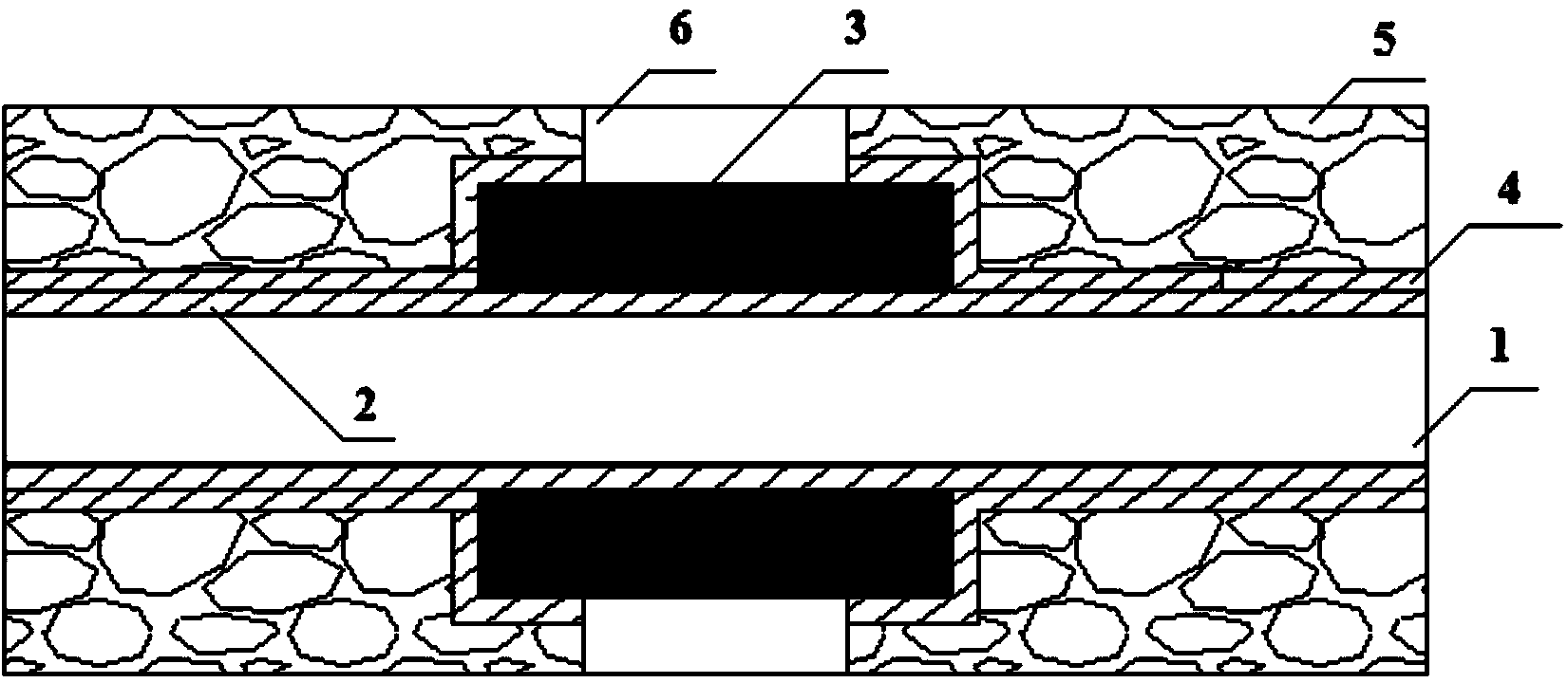
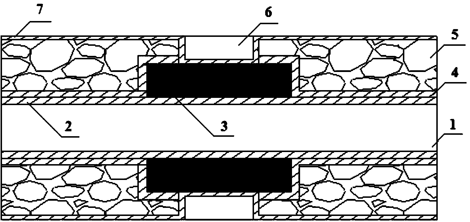
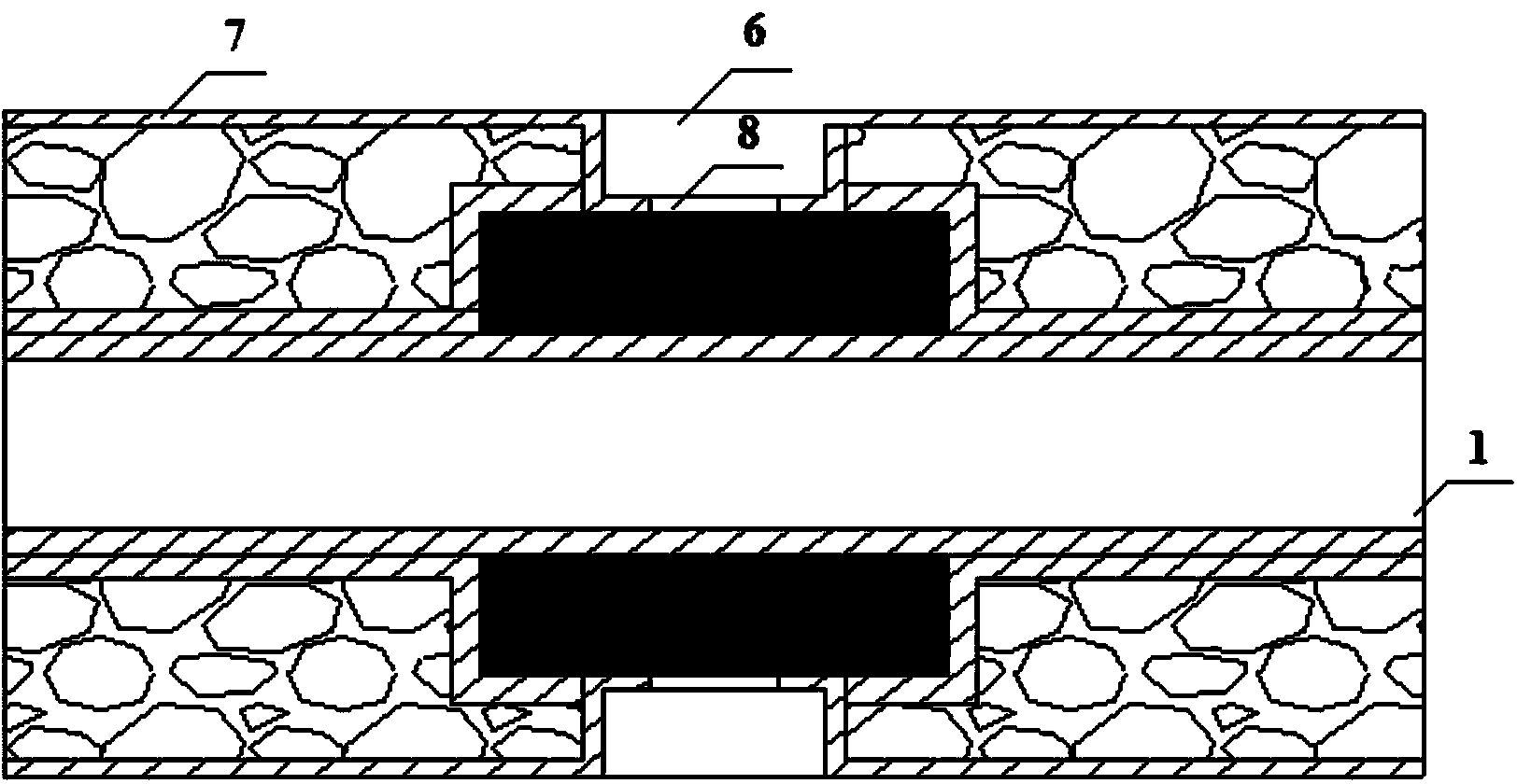
[0031] See figure 1 , The blind hole 6 serves as a channel medium for connecting the multilayer circuit, and penetrates the inner insulating material 5. One end of the blind hole is a partially exposed inner lay...


PUM


Abstract

The invention belongs to the technical field of printed circuit boards and discloses a printed circuit board blind hole manufacturing method. The method comprises the steps of forming a blind hole in a printed circuit board manufactured on an inner line, manufacturing an organic film on the surface of the printed circuit board, forming a connection hole in the organic film on the bottom of the blind hole to enable the inner copper line to be exposed, conducting electroless copper plating on the printed circuit board to form an electroless copper plating layer, conducting electroplating on the electroless copper plating layer to form a porefilling metal electrode and an outer line, and etching the part, not electroplated, of the electroless copper plating layer and arranging an insulating material on the outer line in a press fit mode. According to the method, the surface smoothness of the copper line is improved by making the surface of the copper line coated with the organic film material.

Description

Technical field [0001] The invention relates to the technical field of printed circuit boards, in particular to a method for manufacturing blind holes of printed circuit boards and a structure thereof. Background technique [0002] The blind holes of the printed circuit board, as the connection channel between the multilayer circuits, are of great significance in the design and production process of the printed circuit board. [0003] The conventional blind hole manufacturing process is to drill holes in the insulating material, and conduct hole metallization to connect the upper and lower layers; because the hole metallization is directly performed on the substrate hole wall, the surface smoothness of the copper layer produced is not high, which seriously affects , The quality of signal transmission; surface modification by chemical etching requires high material and equipment investment, which leads to high production costs; at the same time, chemical corrosion modification on th...

Claims


Application Information

Patent Timeline
Patent Type & Authority Applications(China)
IPC IPC(8): H05K3/40H05K1/11
Inventor 于中尧
Owner NAT CENT FOR ADVANCED PACKAGING
Why Eureka
Try Eureka