Organic light-emitting diode display panel and forming method thereof

A technology for light-emitting diodes and display panels, which is applied to instruments, electrical components, and electrical solid-state devices, etc., can solve the problems of aggravating the color shift phenomenon of display panels, the color shift of organic light-emitting diode display panels, and different resonance wavelengths.

Inactive Publication Date: 2014-07-16
XIAMEN TIANMA MICRO ELECTRONICS +1
View PDF7 Cites 27 Cited by
  • Summary
  • Abstract
  • Description
  • Claims
  • Application Information

AI Technical Summary

Problems solved by technology

Although the microcavity effect strengthens the light of a specific wavelength and improves the luminous intensity of the display panel, the resonance wavelength of each angle in the microcavity effect is different, which aggravates the color shift phenomenon of the display panel. Therefore, top emission organic light emitting diodes The problem of color shift at different viewing angles of the display panel is more serious
[0005] For this reason, a new organic light emitting diode display panel and its forming method are needed to solve the color shift problem of the organic light emitting diode display panel

Method used


Image

  • Organic light-emitting diode display panel and forming method thereof
  • Organic light-emitting diode display panel and forming method thereof
  • Organic light-emitting diode display panel and forming method thereof

Examples


Embodiment 1

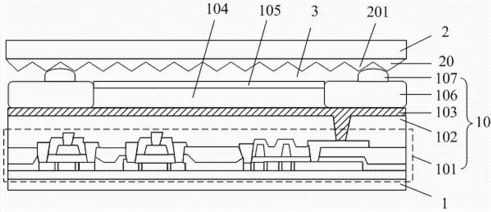
[0027] Embodiment 1 of the present invention provides an OLED display panel, please refer to figure 1 .

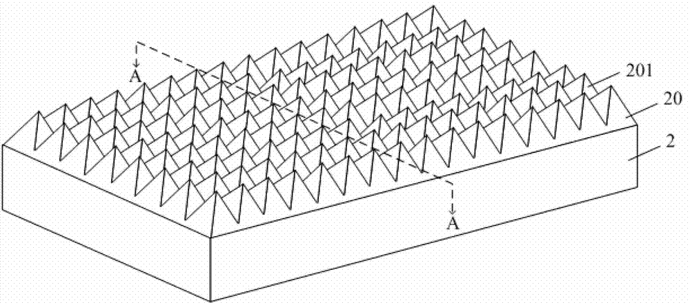
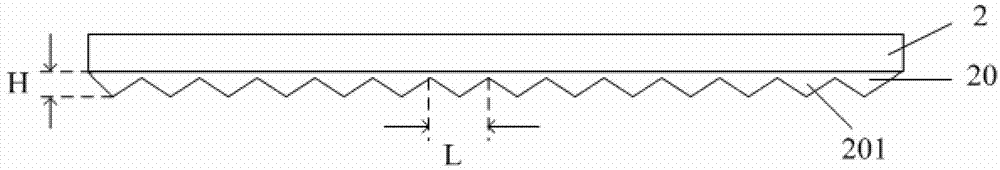
[0028] The organic light emitting diode display panel includes a base substrate 1 and an encapsulation cover plate 2 which are oppositely arranged. The inner surface of the base substrate 1 includes an organic light emitting diode 10 , that is, the organic light emitting diode 10 is located between the base substrate 1 and the package cover 2 . The inner surface of the package cover 2 includes a light-scattering film layer 20 , that is, the light-scattering film layer 20 is located between the package cover 2 and the OLED 10 .

[0029] The organic light emitting diode 10 includes an active electrode part 101 , a protective layer 102 , a reflective electrode layer 103 , an organic light emitting layer 104 , a transparent electrode layer 105 , a pixel defining part 106 and a spacer 107 .

[0030] The active electrode part 101 is located on the inner surface of the base sub...

Embodiment 2

[0051] Embodiment 2 of the present invention provides another organic light emitting diode display panel, please refer to Figure 4 .

[0052] The organic light emitting diode includes a base substrate 4 and a package cover 5 that are oppositely arranged. The inner surface of the base substrate 4 includes an organic light emitting diode 40 , and the inner surface of the package cover 5 includes a light scattering film layer 50 . The organic light emitting diode 40 includes a reflective electrode layer 401 located on the inner surface of the substrate 4, an organic light-emitting layer 402 located on the surface of the reflective electrode layer 401, a transparent electrode layer 403 located on the surface of the organic light-emitting layer 402, and an organic light-emitting layer 403 located on the surface of the transparent electrode layer 403. The passivation protection layer 404, wherein the light generated by the organic light-emitting layer 402 is transmitted through th...


PUM


Abstract

The invention provides an organic light-emitting diode display panel and a forming method thereof. The organic light-emitting diode display panel comprises a substrate base plate and a packaging cover plate which are arranged opposite to each other, an organic light-emitting diode which is located between the substrate base plate and the packaging cover plate, and a light scattering film layer which is located at least one of the inner surface or the outer surface of the packaging cover plate and is capable of conducting scattering on rays emitted by the organic light-emitting diode. Due to the fact that the light scattering film layer can conduct scattering on the rays emitted by the organic light-emitting diode, after the rays are scattered, the scattered rays are emitted from different directions, a looker can see the scattered rays when looking the organic light-emitting diode display panel from different angles, the looker can not see color deviation, and the color-bias phenomenon is eliminated.

Description

technical field [0001] The invention relates to the display field, in particular to an organic light emitting diode display panel and a forming method thereof. Background technique [0002] The organic light emitting diode (OLED) display panel is a self-luminous display panel, which has the advantages of short response time and wide viewing angle range. [0003] The light-emitting layer of the OLED display panel is an organic emitting layer (organic emitting layer, EML), and the organic emitting layer is usually covered with other film layers, so the light generated by the organic light-emitting layer needs to pass through other film layers to enter the atmosphere outside the display. When the light enters the atmosphere through other film layers, it will be refracted. The longer the wavelength of the light, the smaller the refraction angle. Therefore, the refraction angle of red light is smaller than the blue light refraction angle, resulting in the color seen by the human ...

Claims


Application Information

Patent Timeline
Patent Type & Authority Applications(China)
IPC IPC(8): H01L27/32G09F9/33
Inventor 林文晶赵本刚熊志勇
Owner XIAMEN TIANMA MICRO ELECTRONICS
Why Eureka
Try Eureka