A Junction Termination Structure of a Lateral High Voltage Power Semiconductor Device

A technology of power semiconductors and lateral high voltage, applied in the direction of semiconductor devices, electrical components, circuits, etc., can solve problems such as depletion, achieve the effects of optimizing withstand voltage, ensuring withstand voltage, and increasing process steps and costs

Active Publication Date: 2017-05-03
UNIV OF ELECTRONICS SCI & TECH OF CHINA
View PDF3 Cites 0 Cited by
  • Summary
  • Abstract
  • Description
  • Claims
  • Application Information

AI Technical Summary

Problems solved by technology

[0004] What the present invention aims to solve is to propose a junction terminal structure of a lateral high-voltage power semiconductor device for the above-mentioned problem of premature depletion of the drift region at the curvature terminal of the traditional lateral high-voltage power semiconductor device

Method used


Image

  • A Junction Termination Structure of a Lateral High Voltage Power Semiconductor Device
  • A Junction Termination Structure of a Lateral High Voltage Power Semiconductor Device
  • A Junction Termination Structure of a Lateral High Voltage Power Semiconductor Device

Examples


Embodiment 1

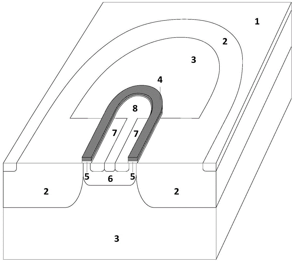
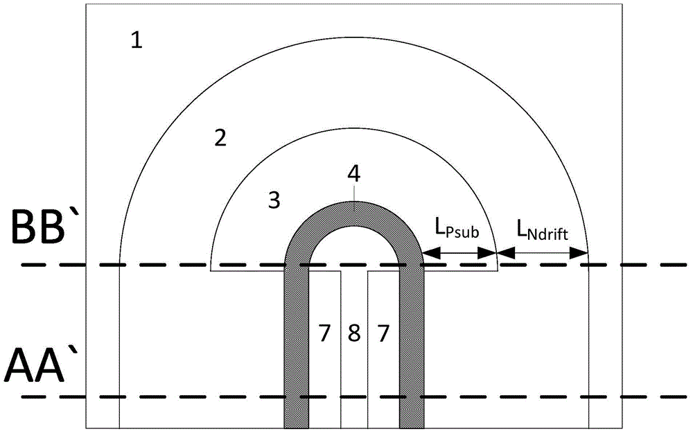
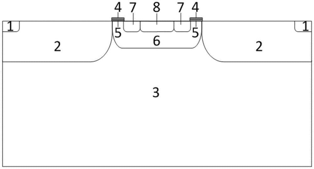
[0033] Such as Figure 10 As shown, this example includes a linear junction terminal structure and a curvature junction terminal structure; the linear junction terminal structure is the same as the active region structure of a lateral high-voltage power semiconductor device, including the drain N + Contact region 1, N-type drift region 2, P-type substrate 3, gate polysilicon 4, gate oxide layer 5, P-well region 6, source N + Contact area 7, source P + Contact region 8; P-well region 6 and N-type drift region 2 are located on the upper layer of P-type substrate 3, wherein P-well region 6 is located in the middle, with N-type drift region 2 on both sides, and P-well region 6 and N-type drift region 2 The drift region 2 is connected; the two sides of the N-type drift region 2 away from the P-well region 6 are the drain N + Contact area 1; drain N + The lateral width of the end of the contact region 1 away from the curvature junction terminal structure is greater than the later...

Embodiment 2

[0038] Such as Figure 11 As shown, the difference between this example and Example 1 is that the original L of the device at the terminal of the curvature junction is kept Psub In the case of the same length, the increase of L Ndrift length, becomes L Ndrift +ΔL, thereby increasing the area of ​​the N-type drift region. When the substrate doping concentration is high, by appropriately increasing the area of ​​the N-type drift region, this can ensure that the withstand voltage of the P-type substrate and the N-type drift region reaches the maximum .

Embodiment 3

[0040] Such as Figure 12 As shown, the difference between this example and Example 1 is that while increasing L Psub length and L Ndrift length, making it L Psub +ΔL 1 and L Ndrift +ΔL 2 , where ΔL 1 with ΔL 2 The sum is equal to ΔL, thereby increasing the area of ​​the P-type substrate region and the N-type drift region at the same time, so that the withstand voltage of the device can be optimized.


PUM


Abstract

The invention relates to the technical field of semiconductor power devices, in particular to a junction terminal structure of a lateral high-voltage power semiconductor device. The invention reduces the total area of ​​the P-type substrate and the N-type drift region of the device at the terminal of the curvature junction, thereby preventing premature depletion of the device at the P-type substrate region and ensuring the withstand voltage of the device at the terminal of the curvature junction. The beneficial effect of the present invention is that it can significantly reduce the impact of the curvature junction terminal on the withstand voltage of the entire device, so that the electric field of the device in the transition region will not be too large, and the device's withstand voltage can be improved by changing the area of ​​the drift region or the P-type substrate. The voltage is optimized to ensure the withstand voltage of the device. The invention is especially suitable for junction termination structures of lateral high-voltage power semiconductor devices.

Description

technical field [0001] The invention relates to the technical field of semiconductor power devices, in particular to a junction terminal structure of a lateral high-voltage power semiconductor device. Background technique [0002] With the increasing electrification of industry, the requirements for high voltage and high current devices are getting higher and higher. In order to improve the withstand voltage of the device, various junction termination structures have emerged to meet the withstand voltage requirements of the device. [0003] The development of high-voltage power integrated circuits is inseparable from the integration of lateral high-voltage power semiconductor devices. Lateral high-voltage power semiconductor devices are usually closed structures, including circular, racetrack and interdigitated structures. For the closed racetrack structure and interdigitated structure, there will be small curvature terminations in the curved part and the fingertip part, a...

Claims


Application Information

Patent Timeline
Patent Type & Authority Patents(China)
IPC IPC(8): H01L29/06H01L29/78
CPCH01L29/063
Inventor 乔明文帅张昕齐钊薛腾飞吴文杰张波
Owner UNIV OF ELECTRONICS SCI & TECH OF CHINA
Why Eureka
Try Eureka