
A silicon-based thin epitaxial single-resurf level-shift structure

A level shifting and epitaxy technology, which is applied in the direction of circuits, electrical components, and electrical solid devices, can solve problems such as early breakdown of devices, large lateral diffusion of junction isolation, and long thermal process time, so as to reduce the impact of device withstand voltage , The effect of increasing the breakdown voltage and increasing the length

Active Publication Date: 2018-04-06
UNIV OF ELECTRONICS SCI & TECH OF CHINA
View PDF6 Cites 0 Cited by
  • Summary
  • Abstract
  • Description
  • Claims
  • Application Information

AI Technical Summary

Problems solved by technology

[0005] Aiming at the problems existing in the background technology, the present invention proposes a silicon-based thin epitaxy single RESURF level shift structure to solve the shortcomings of traditional thick epitaxy technology such as long thermal process time, large lateral diffusion of junction isolation, and blurred lithographic marks after thick epitaxy.
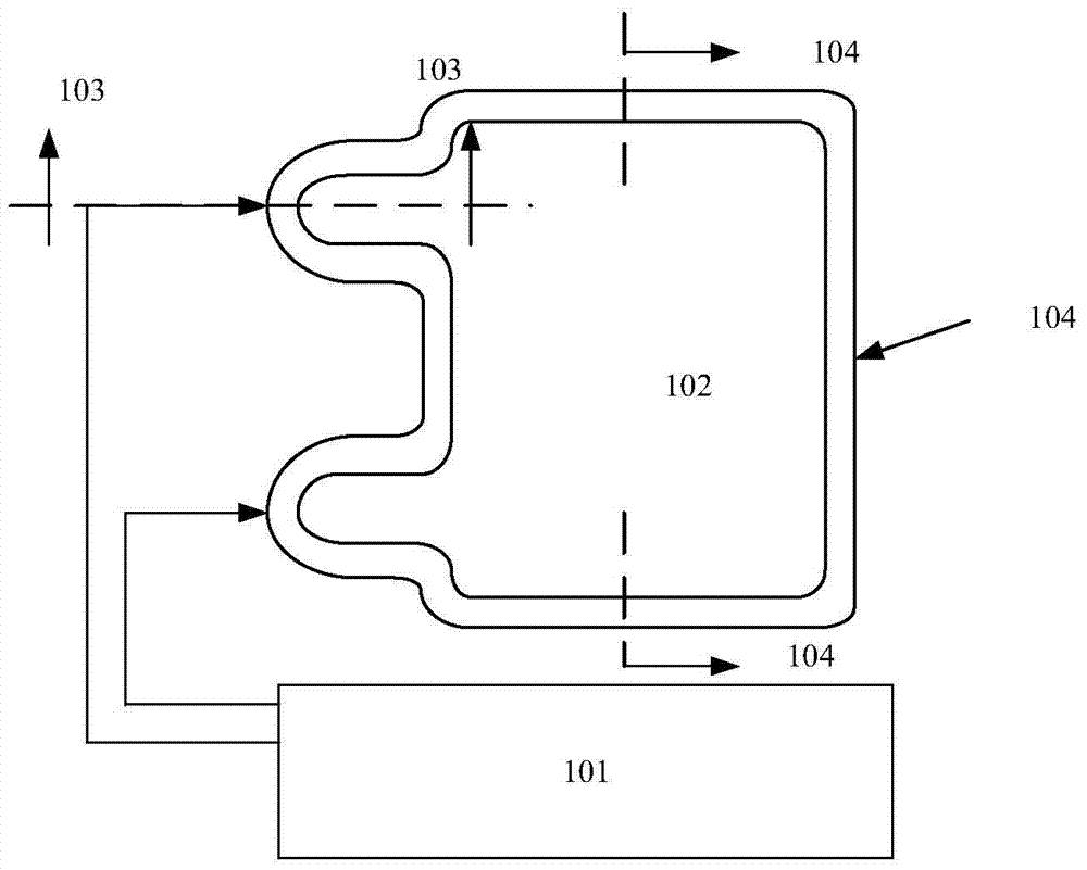
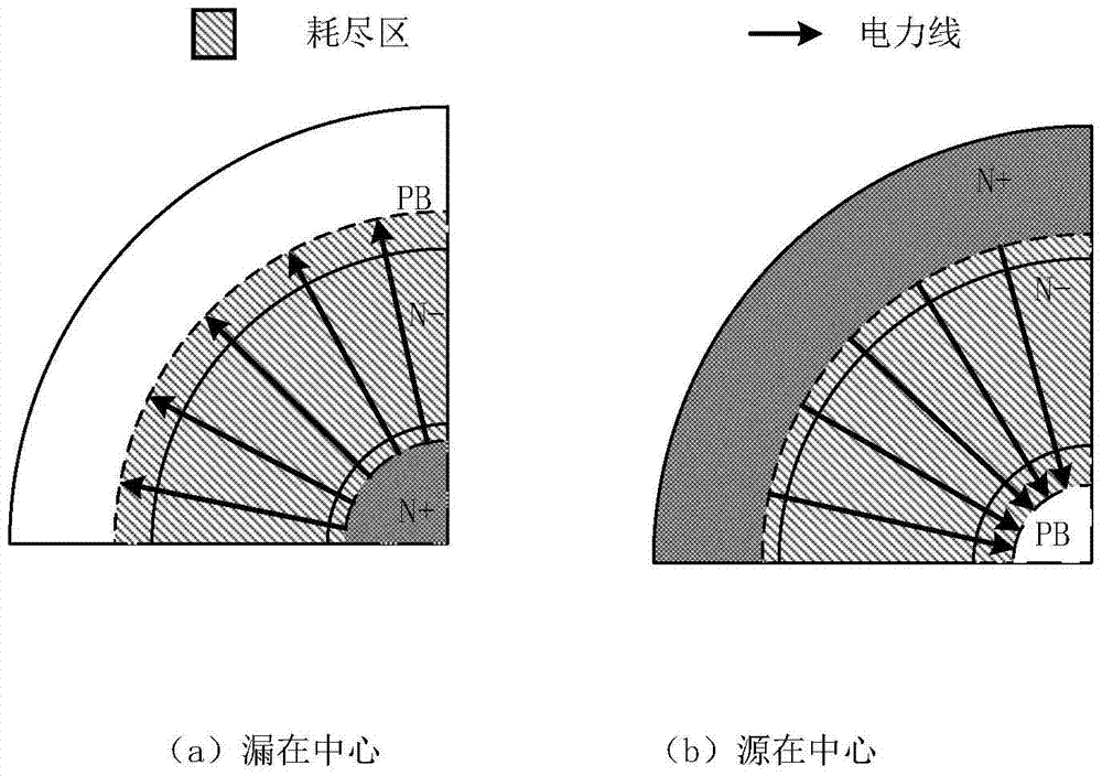
[0007] In order to solve the problem of early breakdown of the device caused by the thin epitaxial curvature effect, the present invention proposes a silicon-based thin epitaxial single RESURF level shift structure, such as Figure 4 As shown, it includes a high-end circuit 402 based on a floating ground, a terminal 403, an LDMOS 401, a first curved area 405, and a second curved area 404; for the first curved area 405, the curvature radius of the drain is increased to meet the withstand voltage requirement; For the second bend region 404, increase the length of the drift region in the second bend region. The optimized drift region length will weaken the electric field concentration of the curvature junction, avoid the concentration of electric field lines at the source end, and obtain a longer withstand voltage layer , to avoid premature breakdown, thereby increasing the breakdown voltage in the bend area

Method used


Image

  • A silicon-based thin epitaxial single-resurf level-shift structure
  • A silicon-based thin epitaxial single-resurf level-shift structure
  • A silicon-based thin epitaxial single-resurf level-shift structure

Examples


Embodiment 1

[0045] Figure 10 A schematic diagram of the silicon-based thin epitaxial single RESURF level shift structure provided by Embodiment 1 of the present invention. Including a pair of LDMOS 401, a high-end circuit 402 based on floating ground, a terminal 403, and two curved areas 404 and 405; for the first curved area 405, the curvature radius of the drain is increased to meet the withstand voltage requirement; for the second curved area In area 404, when side H remains unchanged, the radius of curvature of the arc on side B is reduced, and at the same time, the drift area in the straight track area gradually changes to the drift area in the curve area; and the radius of curvature of side B cannot be too low, and the basic withstand voltage requirements must be guaranteed.

Embodiment 2

[0047] Figure 11 It is a schematic diagram of the silicon-based thin epitaxial single RESURF level shift structure provided by Embodiment 2 of the present invention. Including a pair of LDMOS 401, a high-end circuit 402 based on floating ground, a terminal 403, and two curved areas 404 and 405; for the first curved area 405, the curvature radius of the drain is increased to meet the withstand voltage requirement; for the second curved area zone 404, increasing the radius of curvature of the B side and H side arcs at the same time, and the radius of curvature of the H side is much greater than that of the B side, so as to ensure that the length of the drift zone of the second curve zone is increased; at the same time, the drift zone of the straight track zone Fade to corner zone drift zone.

Embodiment 3

[0049] Figure 12 It is a schematic diagram of the silicon-based thin epitaxial single RESURF level shift structure provided by Embodiment 3 of the present invention. Including a pair of LDMOS 401, a high-end circuit 402 based on floating ground, a terminal 403, and two curved areas 404 and 405; for the first curved area 405, the curvature radius of the drain is increased to meet the withstand voltage requirement; for the second curved area In area 404, when increasing the radius of curvature of the arc on the H side, the radius of curvature of the arc on the B side is reduced to ensure that the length of the drift zone in the second curve area is increased; Press demand; at the same time, the drift zone in the straight track area gradually changes to the drift zone in the curve area.

[0050] The invention is also applicable to the thin epitaxial double RESURF structure, only needing to add ptop layer.

[0051] The invention is equally applicable in thick epitaxial structur...


PUM


Abstract

The invention relates to a silicon base thin epitaxial single RESURF level displacement structure, which belongs to the technical field of semiconductor power devices. Including floating ground-based high-end circuits, terminals, LDMOS, the first bend area, and the second bend area; for the first bend area, increase the curvature radius of the drain to meet the withstand voltage requirements; for the second bend area, increase The length of the drift zone in the second bend area is large, and the optimized drift zone length will weaken the electric field concentration of the curvature junction, avoid the concentration of electric field lines at the source end, and will obtain a longer voltage withstand layer to avoid early breakdown, thereby improving bend channel breakdown voltage. The level displacement structure of the present invention can prevent the electric field on the surface of the curvature terminal with the source in the center from being too concentrated, and reduce the influence of the curvature on the withstand voltage of the device; compared with the existing curvature terminal processing method, the present invention does not introduce a new version or The process flow is low in cost, and the process is compatible with the standard CMOS process flow, which realizes the integration of the level-shift structure of the high-voltage integrated circuit.

Description

technical field [0001] The invention belongs to the technical field of semiconductor power devices, and in particular relates to a silicon-based thin epitaxial single RESURF level displacement structure. Background technique [0002] A high-voltage integrated circuit is composed of a low-voltage area and a high-voltage area. When the high-voltage and low-voltage devices are integrated on the same chip in a power integrated circuit, in order to realize the function of transmitting the low-end control signal to the high-end, it is often unavoidable that there will be hundreds of volts High-voltage interconnect lines HVI with even thousands of volts cross over low-voltage devices, partial areas on the surface of isolation regions, or low-voltage portions of high-voltage devices. The high potential on the interconnect lines affects the electric field distribution on the Si surface at the high-voltage junction termination, reducing its withstand voltage. [0003] High-voltage po...

Claims


Application Information

Patent Timeline
Patent Type & Authority Patents(China)
IPC IPC(8): H01L27/06H01L29/06
Inventor 乔明张晓菲王裕如代刚张波
Owner UNIV OF ELECTRONICS SCI & TECH OF CHINA
Learn More