Quantum dot and graphene photosensitive field-effect transistor and manufacturing method thereof

A technology of ene photosensitive field and field effect tube, which is applied in the direction of final product manufacturing, sustainable manufacturing/processing, electrical components, etc., can solve the problems affecting the stability of the electrical characteristics of field effect tubes, and achieve low cost, high responsiveness, The effect of high reliability and stability

Inactive Publication Date: 2014-07-23
TIANJIN UNIV
View PDF2 Cites 13 Cited by
  • Summary
  • Abstract
  • Description
  • Claims
  • Application Information

AI Technical Summary

Problems solved by technology

[0007] The purpose of the present invention is to solve the problem that the small size field effect tube is affected by the stability of the electrical characteristics of the field effect tube due to the constraints of processing

Method used


Image

  • Quantum dot and graphene photosensitive field-effect transistor and manufacturing method thereof
  • Quantum dot and graphene photosensitive field-effect transistor and manufacturing method thereof
  • Quantum dot and graphene photosensitive field-effect transistor and manufacturing method thereof

Examples


Embodiment

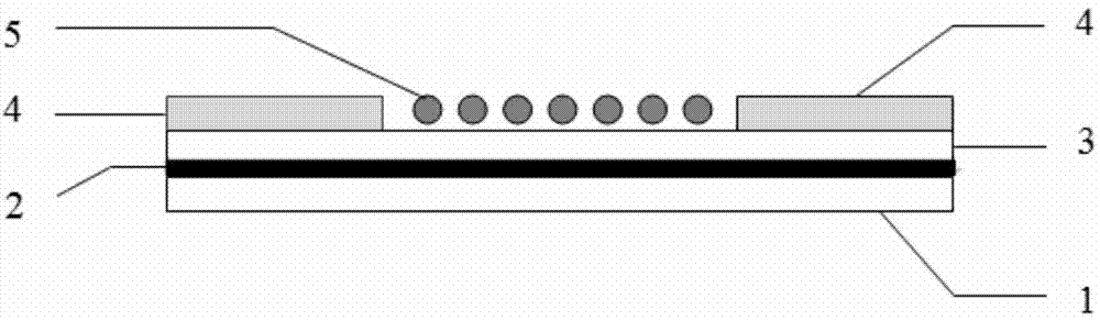
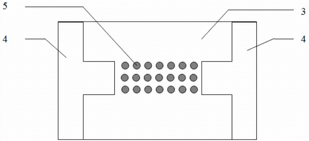
[0044] 1. Quantum dot / graphene photosensitive field effect tube structure

[0045] Such as figure 1 As shown, the structures of quantum dots and graphene field effect transistors are as follows from bottom to top: silicon-based substrate layer 1, silicon dioxide layer 2, graphene layer 3, electrode layer 4 and quantum dots 5.

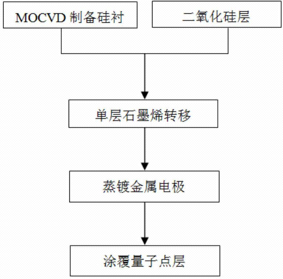
[0046] 2. Preparation of quantum dot / graphene photosensitive field effect tube

[0047]1. Preparation of silicon-based substrate layer and silicon dioxide layer

[0048] The silicon-based substrate layer was prepared by MOCVD method. The bottom layer of the substrate is highly doped single crystal silicon with a thickness of 3 μm, and the upper layer of the silicon base substrate is an oxidized silicon dioxide layer with a thickness of 300±5nm.

[0049] 2. Preparation of graphene layer

[0050] What the preparation of graphene layer adopted in this embodiment is the wet transfer method, and concrete process is as follows:

[0051] 1. Protect the si...


PUM

PropertyMeasurementUnit
Thicknessaaaaaaaaaa

Abstract

Provided are a quantum dot and graphene photosensitive field-effect transistor and a manufacturing method thereof. The field-effect transistor structurally and sequentially includes a silicon-based substrate layer, a silicon dioxide layer, a graphene layer, an electrode layer and a quantum dot layer located on the upper portion of the graphene layer and in a middle channel of the electrode layer. The manufacturing process of the field-effect transistor is as follows: firstly, the silicon-based substrate layer and the silicon dioxide layer are prepared in an existing mature technique; secondly, the graphene layer is prepared on the upper portion of the silicon dioxide layer in a wet process transfer method, then the electrode layer including a source electrode and a drain electrode is prepared in a multisource organic vapor phase deposition method, and ultimately, the quantum dot layer is prepared in the middle channel of the electrode layer in a layer-by-layer covering method. The quantum dot layer is ingeniously applied to the middle channel area of the electrode layer in the method that the electrodes are evaporated first and then the quantum dot layer is applied, the quantum dot layer is attached to the upper portion of the graphene layer to form physical composition of quantum dots and graphene materials. The field-effect transistor has high responsivity for incident light of an infrared band.

Description

technical field [0001] The invention belongs to the field of semiconductor materials and photoelectric devices, and relates to a light-sensitive field-effect tube, in particular to an infrared-band light-sensitive field-effect tube based on quantum dots / graphene. Background technique [0002] The traditional field effect transistor realizes its function by using the gate voltage to control the number of carriers in the conduction channel. The production method is relatively mature, and the device molding is relatively stable. From the point of view of its working process, the source and drain of the field effect transistor are interchangeable, that is, the source and drain of the field effect transistor are symmetrical, which avoids the reverse connection during actual use. The possibility of circuit damage is not easy for ordinary transistors. Second, field effect transistors have a low noise figure and are highly resistant to radiation. [0003] Under the background th...

Claims


Application Information

Patent Timeline
IPC IPC(8): H01L31/09H01L31/0352H01L31/18
CPCH01L31/035218H01L31/112H01L31/18Y02P70/50
Inventor 张雅婷王茂榕宋效先金露凡王海艳
Owner TIANJIN UNIV
Why Eureka
Try Eureka