Full-duplex and half-duplex converter and conversion method
A half-duplex and full-duplex technology, which is applied in the direction of duplex signal operation, can solve the problems of data loss and bit error rate, and achieve the effect of ensuring accuracy and solving communication compatibility problems
- Summary
- Abstract
- Description
- Claims
- Application Information
AI Technical Summary
Problems solved by technology
Method used
Image
Examples
specific Embodiment approach 1
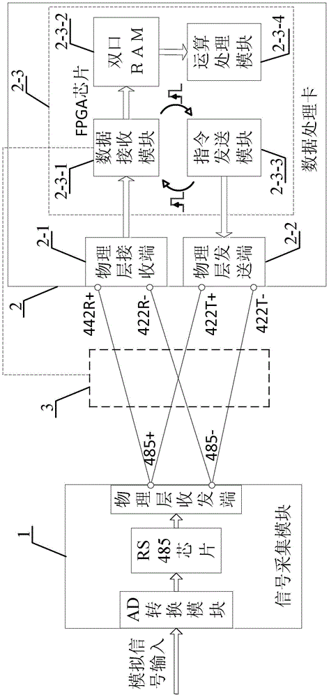
[0043] Specific implementation mode one: combine figure 1 Describe this embodiment, the full-duplex and half-duplex converter described in this embodiment includes a half-duplex signal acquisition module 1, a full-duplex data processing module 2 and a tri-state gate integrated circuit 3, the full-duplex Data processing module 2 comprises physical layer receiving end 2-1, physical layer sending end 2-2 and FPGA chip 2-3;
[0044] Described half-duplex signal acquisition module 1 adopts RS485 chip to realize, and described physical layer receiving end 2-1 and physical layer sending end 2-2 all adopt 422 serial port driver modules to realize;
[0045] The 422R+ port and the 422R- port of the physical layer receiving end 2-1 are respectively connected to the data signal output + port and the data signal output - port of the tri-state gate integrated circuit 3, and the 422T+ port and the 422T- port of the physical layer sending end 2-2 are respectively Connect the command signal i...
specific Embodiment approach 2
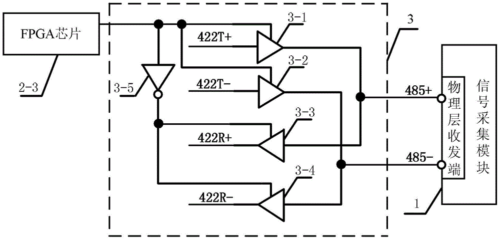
[0064] Specific implementation mode two: combination figure 1 and figure 2 This embodiment is described. This embodiment is a further limitation of the full-duplex and half-duplex converter described in Embodiment 1. In this embodiment, the tri-state gate integrated circuit 3 includes a first tri-state gate 3 -1, the second tri-state gate 3-2, the third tri-state gate 3-3, the fourth tri-state gate 3-4 and the NOT gate 3-5;
[0065] The input end of the NOT gate 3-5, the enable signal end of the first tri-state gate 3-1 and the enable signal end of the second tri-state gate 3-2 are connected together as the tri-state gate integrated circuit 3 The enable signal input end, the output end of the NOT gate 3-5 is simultaneously connected to the enable signal end of the third tri-state gate 3-3 and the enable signal end of the fourth tri-state gate 3-4;
[0066] The input end of the first tri-state gate 3-1 is connected to the 422T+ port of the physical layer sending end 2-2, the...
specific Embodiment approach 3
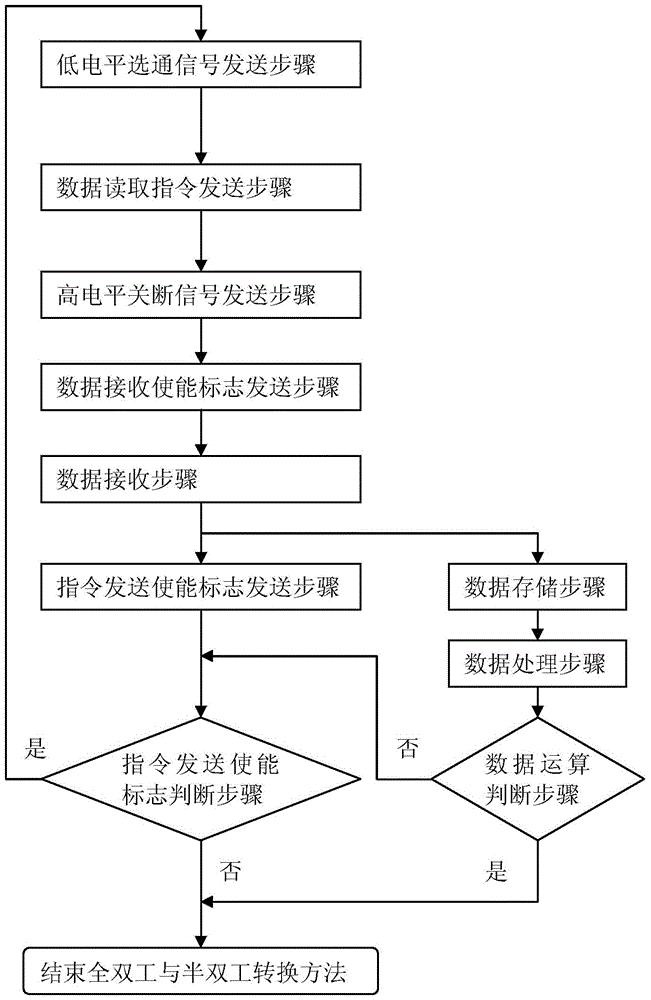
[0070] Specific implementation mode three: combination figure 1 and image 3 Describe this embodiment, the full-duplex and half-duplex conversion method described in this embodiment is realized based on the following conversion device: the conversion device includes a half-duplex signal acquisition module 1, a full-duplex data processing module 2 and three State gate integrated circuit 3, described full-duplex data processing module 2 comprises physical layer receiving end 2-1, physical layer sending end 2-2 and FPGA chip 2-3;
[0071] Described half-duplex signal acquisition module 1 adopts RS485 chip to realize, and described physical layer receiving end 2-1 and physical layer sending end 2-2 all adopt 422 serial port driver modules to realize;
[0072] The 422R+ port and the 422R- port of the physical layer receiving end 2-1 are respectively connected to the data signal output + port and the data signal output - port of the tri-state gate integrated circuit 3, and the 422T...
PUM
 Abstract
Description
Claims
Application Information


