

Nanoscale three-state resistive random access memory and preparation method thereof
A three-state resistance and memory technology, applied in electrical components and other directions, can solve the problems of short holding time and poor switching performance of multi-resistance resistive devices, and achieve the effect of significant switching effect, good performance, and concentrated resistance cumulative probability distribution.
- Summary
- Abstract
- Description
- Claims
- Application Information
AI Technical Summary
Problems solved by technology
Method used
Image

Examples
Embodiment 1
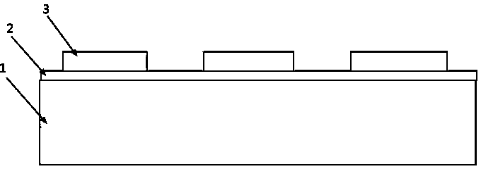
[0036] Example 1: Preparation of a three-state resistive memory with Ag / nc-Si:H / Pt structure
[0037] 1. In Pt / Ti / SiO 2 Deposition of nc-Si:H film on / Si substrate:
[0038] 1. Selection and processing of substrate materials: choose Pt / Ti / SiO 2 / Si as the substrate, first place it in acetone and ultrasonically clean it for 10 minutes, then put it in alcohol and clean it ultrasonically for 10 minutes, then take it out with a plastic clip and put it in deionized water and clean it ultrasonically for 5 minutes, then take it out and clean it with nitrogen (N 2 ) and blow dry.
[0039] 2. Put in the substrate and vacuumize: open the chamber of the PECVD equipment (radio frequency plasma enhanced chemical vapor deposition system), and put the cleaned substrate (ie Pt / Ti / SiO 2 / Si substrate) placed on the substrate table of the PECVD equipment cavity and fixed, then close the cavity, set the plate spacing to 2cm according to the conventional operation requirements, then turn on th...
Embodiment 2
[0047] Embodiment 2: the Raman spectrogram of the nc-Si:H thin film prepared in embodiment 1
[0048] Detect the Raman spectrogram of the nc-Si:H film of the memory element (i.e. the three-state resistive memory of Ag / nc-Si:H / Pt structure) prepared in Example 1 for analysis, the results are as follows Figure 5 shown. Figure 5 , the peak is located near 500cm-1, by Figure 5 It can be calculated that the crystallization rate of nc-Si:H film is 42.4%.
Embodiment 3
[0049] Example 3: High Resolution Transmission Electron Microscopy (HRTEM) image of the nc-Si:H thin film prepared in Example 1
[0050] Use high-resolution transmission electron microscopy (HRTEM) to scan the high-resolution transmission electron microscope (HRTEM) figure of the nc-Si:H film of the memory element prepared in Example 1, and the results are as follows Image 6 shown. Depend on Image 6 It can be seen that in the uniform amorphous network, there are small grains around the amorphous matrix, and the grains gather together in the amorphous matrix to form spherical nanoparticles.
PUM
 Abstract
Description
Claims
Application Information