In cell touch panel and display device

An embedded touch screen, consistent technology, applied in optics, instrumentation, electrical digital data processing, etc., can solve the problems of large number of peripheral traces, unfavorable narrow frame design, large touch blind area, etc., to reduce the disadvantages of narrow The probability of occurrence of problems such as frame design and relatively large touch blind area, the reduction of the number of wires, and the effect of reducing the number of wires

Active Publication Date: 2014-09-03
BOE TECH GRP CO LTD +1
View PDF5 Cites 57 Cited by
  • Summary
  • Abstract
  • Description
  • Claims
  • Application Information

AI Technical Summary

Problems solved by technology

[0005] And, in concrete implementation, the quantity of self-capacitance electrode can be very much, be 5mm*5mm as example with the occupied area of ​​each self-capacitance electrode, 5 inches liquid crystal screen just needs 264 self-capacitance electrodes, if each If the self-capacitance electrode design is smaller, there will be more self-capacitance electrodes, so that the number of wires connected to the self-capacitance electrodes is very large, which will cause some problems. There will also be a large number of peripheral traces connected to the wires in one-to-one correspondence, which is not conducive to the narrow frame design; or, when the wires and self-capacitance electrodes are arranged on the same layer, the large number of wires will cause a relatively large touch blind area
[0006] To sum up, at present, the number of self-capacitance electrodes in the self-capacitance touch screen is very large, so that the number of wires connected to the self-capacitance electrodes is also very large, which will cause problems such as unfavorable narrow frame design and relatively large touch blind area.

Method used


Image

  • In cell touch panel and display device
  • In cell touch panel and display device
  • In cell touch panel and display device

Examples


Embodiment 1

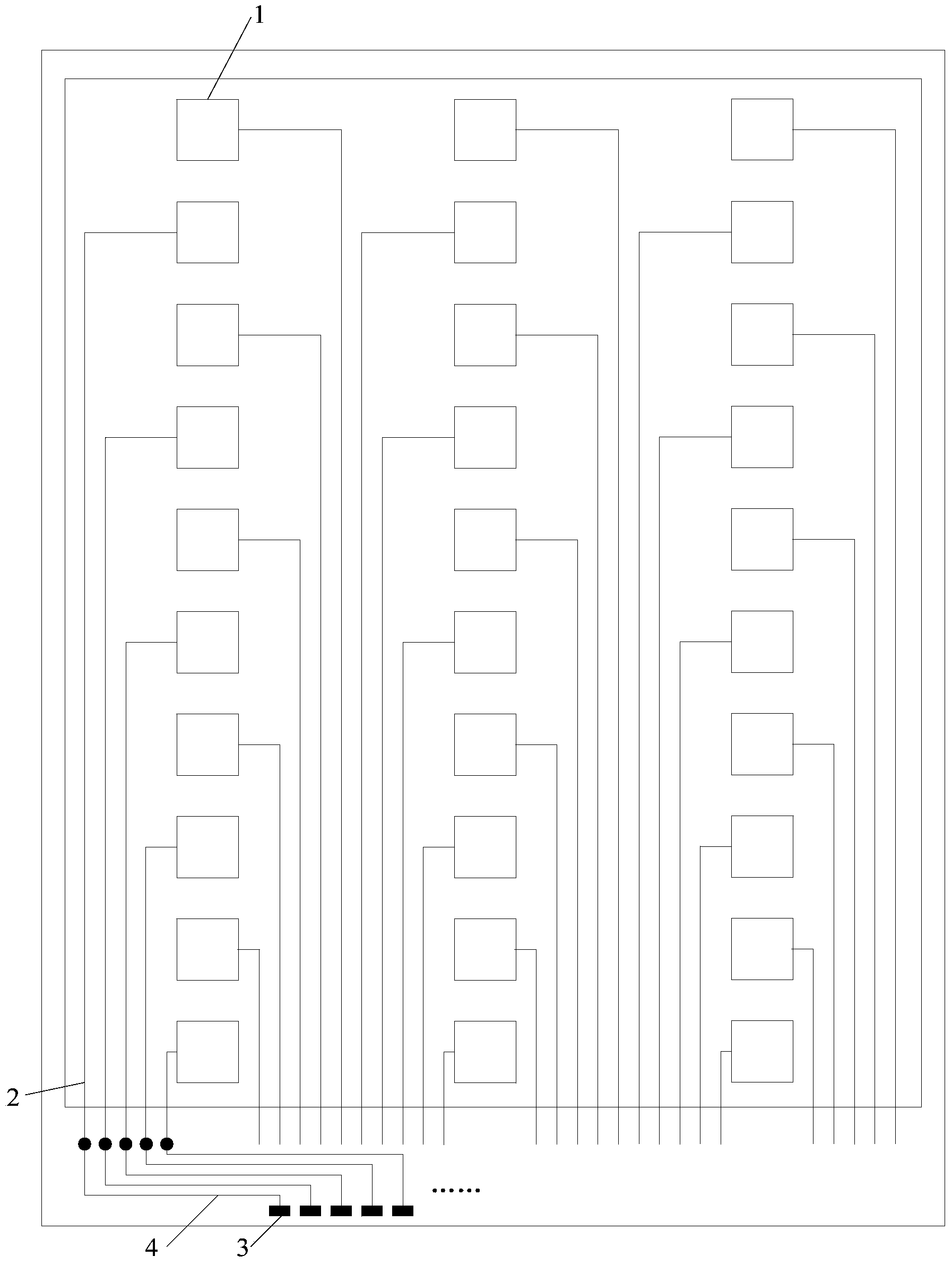
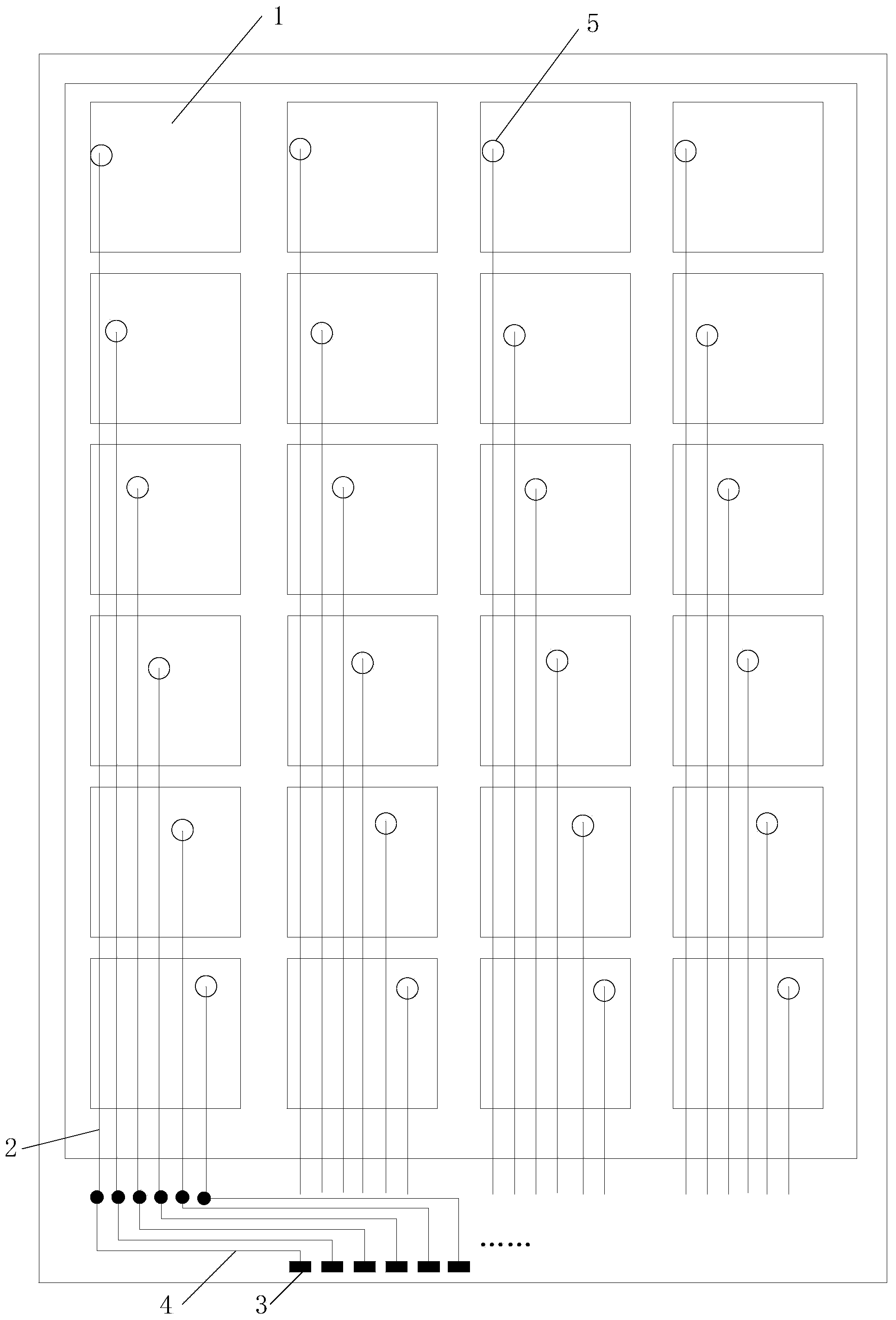
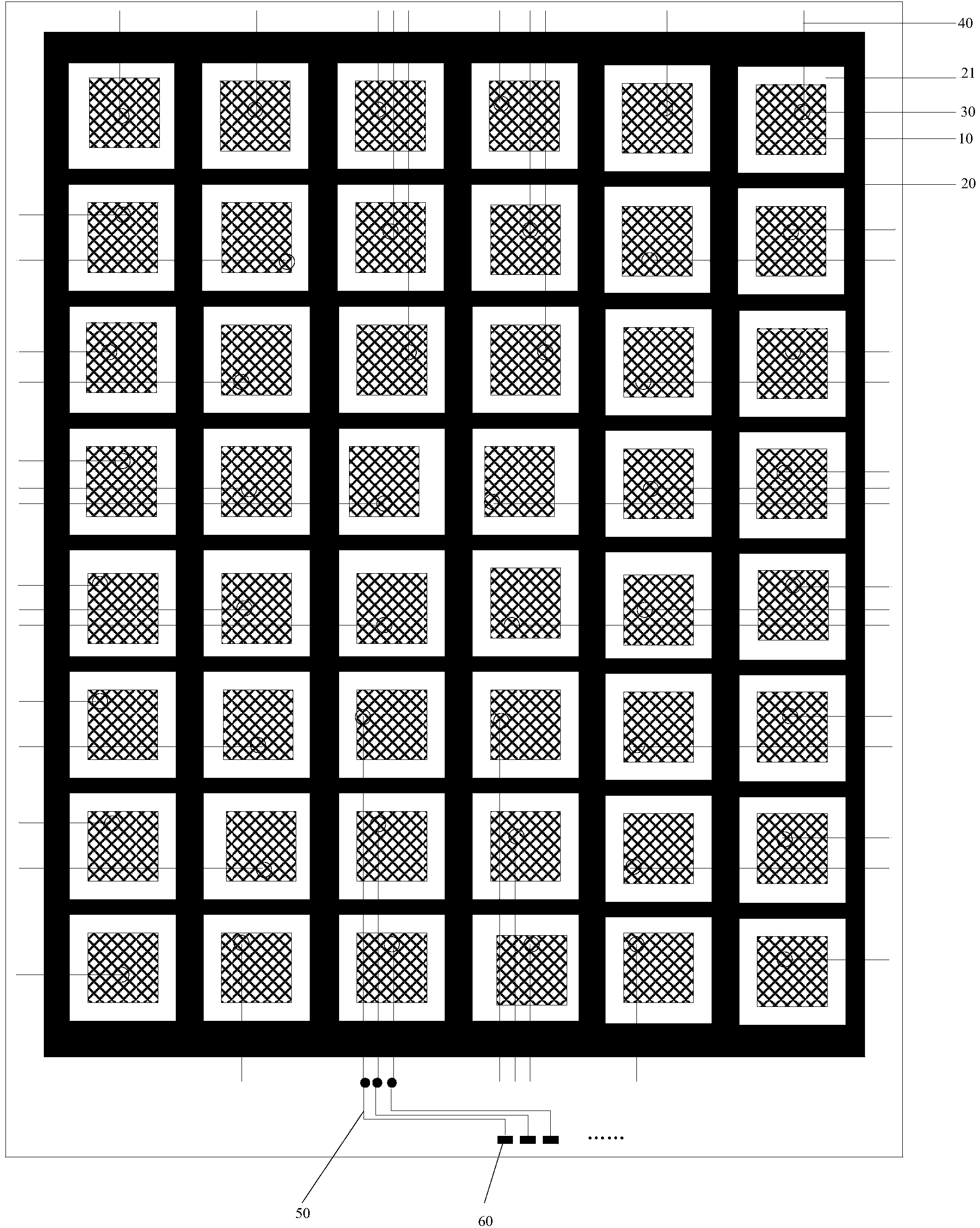
[0120] In the first embodiment of the present invention, the combination of Figure 2a , to explain the principle of solving the problem of reducing the number of self-capacitance electrodes in the embodiment of the present invention.

[0121] Such as Figure 2a As shown, the embedded touch screen of the embodiment of the present invention includes:

[0122] A conductive layer 20 comprising a plurality of hollow areas 21 arranged in a matrix; wherein, Figure 2a It is illustrated by taking 8 rows and 6 columns and a total of 48 hollow areas 21 as an example;

[0123] A plurality of self-capacitance electrodes 10 arranged on the same layer as the conductive layer 20 and mutually insulated from the conductive layer 20; wherein, each of the hollowed out regions 21 is provided with one self-capacitance electrode 10; Figure 2a It is illustrated by taking a total of 48 self-capacitance electrodes 10 in 8 rows and 6 columns as an example;

[0124] A plurality of non-intersecting...


PUM


Abstract

The invention relates to the field of the touch technology, in particular to an in cell touch panel and a display device. By the adoption of the in cell touch panel and the display device, the number of wires in the in cell touch panel is reduced, and the probability of the problems that narrow bezel design cannot be achieved easily and the touch dead zone is large is reduced to a certain extent. The in cell touch panel comprises an upper substrate and a lower substrate which are arranged oppositely. The in cell touch panel further comprises a conductive layer, a plurality of self-capacitance electrodes, a plurality of wires and a touch detecting chip, wherein the conductive layer is arranged on the side, facing the lower substrate, of the upper substrate or on the side, facing the upper substrate, of the lower substrate, the conductive layer comprises a plurality of hollowed-out areas which are arranged in an array mode, the self-capacitance electrodes and the conductive layer are arranged on the same layer and are mutually insulated, each hollowed-out area is provided with the corresponding self-capacitance electrode, the wires are electrically connected with the self-capacitance electrodes, and the touch detecting chip is electrically connected with the wires.

Description

technical field [0001] The present invention relates to the field of touch technology, in particular to an embedded touch screen and a display device. Background technique [0002] With the rapid development of display technology, touch screen panels (Touch Screen Panels) have gradually spread in people's lives. At present, touch screens can be divided into three types according to their composition structure: Add on Mode Touch Panel, On Cell Touch Panel, and In Cell Touch Panel; ) type touch screen can be divided into: mutual capacitance touch screen and self capacitance touch screen. As for the self-capacitance touch screen, due to its high accuracy of touch sensing and relatively high signal-to-noise ratio, it is favored by major panel manufacturers. [0003] At present, the self-capacitance touch screen uses the principle of self-capacitance to detect the touch position of the finger. Specifically, a plurality of self-capacitance electrodes set on the same layer and in...

Claims


Application Information

Patent Timeline
Patent Type & Authority Applications(China)
IPC IPC(8): G06F3/044
CPCG06F3/0412G06F3/04164G06F3/04166G06F3/0443G06F3/0448G06F2203/04112G02F1/1333G06F2203/04111
Inventor 杨盛际董学王海生薛海林刘英明赵卫杰丁小梁刘红娟李昌峰
Owner BOE TECH GRP CO LTD
Why Eureka
Try Eureka