Charge and discharge control circuit and battery device
一种充放电控制、充放电的技术,应用在电池电路装置、电路装置、紧急保护电路装置等方向,达到防止电压上升、提高安全性的效果
- Summary
- Abstract
- Description
- Claims
- Application Information
AI Technical Summary
Problems solved by technology
Method used
Image

Examples
no. 1 approach
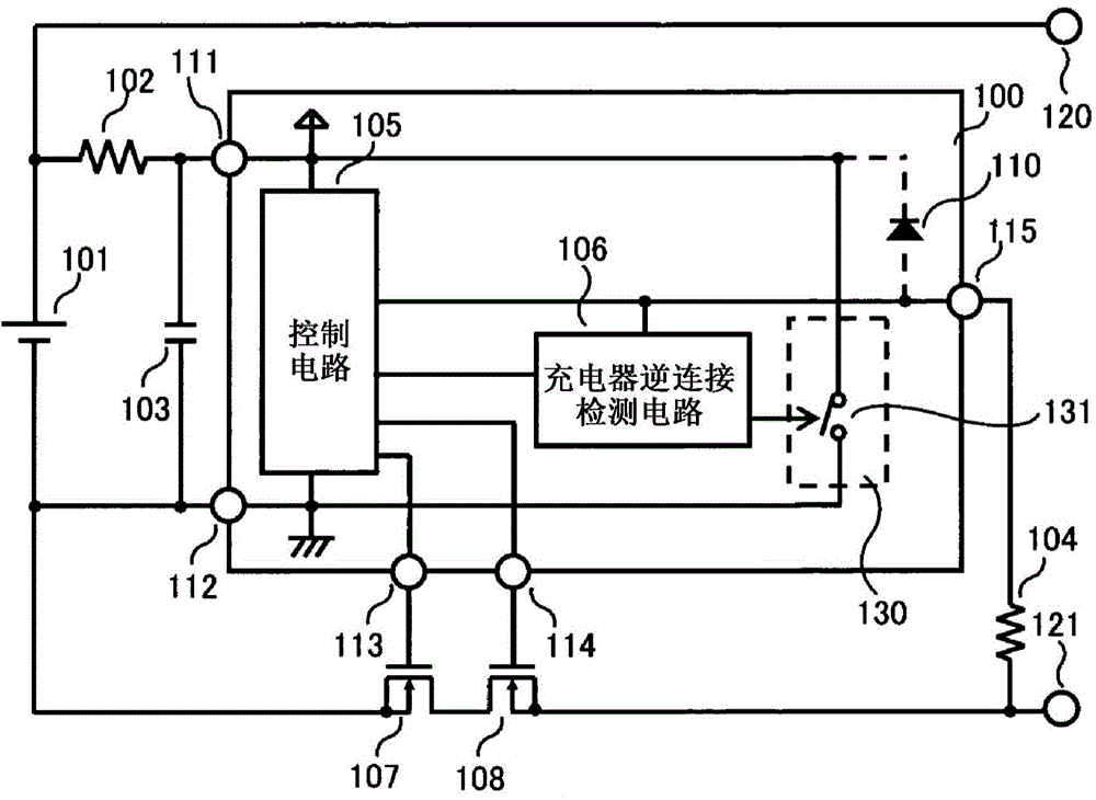
[0022] figure 1 It is a circuit diagram of the charge and discharge control circuit and the battery device of the first embodiment.
[0023] The charge and discharge control circuit and the battery device of the first embodiment are composed of a secondary battery 101, resistors 102, 104, a capacitor 103, a discharge control NchFET transistor 107, a charge control NchFET transistor 108, a charge and discharge control circuit 100, and an external terminal 120, 121 composition. Charge and discharge control circuit 100 is composed of control circuit 105 , charger reverse connection detection circuit 106 , current consumption increasing circuit 130 , VDD terminal 111 , VSS terminal 112 , DO terminal 113 , CO terminal 114 and VM terminal 115 . The consumption current increasing circuit 130 is composed of a switch circuit 131 .
[0024] The positive electrode of the secondary battery 101 is connected to the external terminal 120 and the resistor 102 , and the negative electrode i...
no. 2 approach
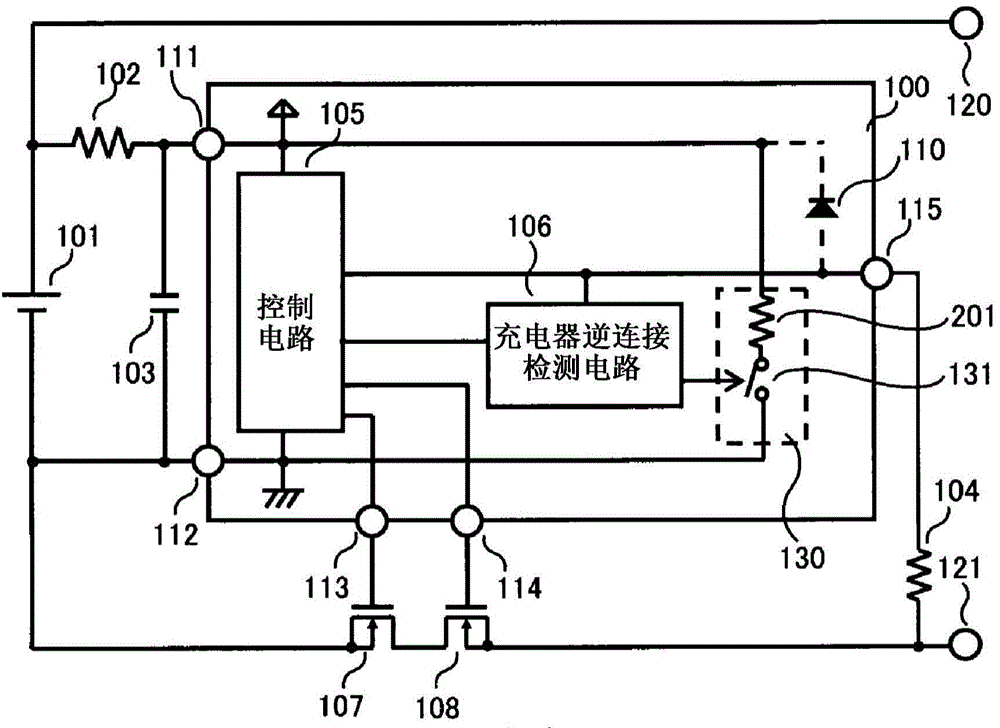
[0036] figure 2 It is a circuit diagram of the charging and discharging control circuit and the battery device of the second embodiment.
[0037] The difference from the first embodiment is that a resistor 201 as an impedance element is inserted between the switch circuit 131 and the VDD terminal 111 . Others are the same as the first embodiment.
[0038] Operations of the charge and discharge control circuit and the battery device according to the second embodiment will be described.
[0039] The operation of the overcharged state, overdischarged state, overcurrent state, and charger reverse connection detection circuit 106 is the same as that of the first embodiment. When the charger reverse connection state is reached and the charger reverse connection detection circuit 106 turns on the switch circuit 131 , the consumption current increasing circuit 130 operates, and the current value Ids flows from the VDD terminal 111 to the VSS terminal 112 . This current Ids is adju...
no. 3 approach
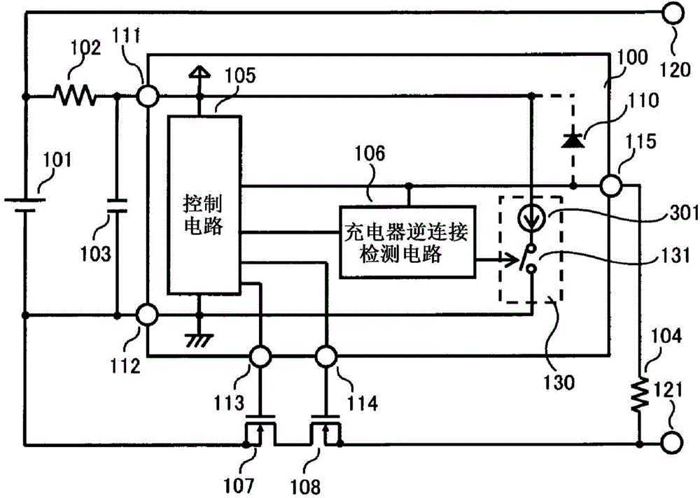
[0043] image 3 It is a circuit diagram of the charging and discharging control circuit and the battery device of the third embodiment.
[0044] The difference from the second embodiment is that the resistor 201 is changed to a constant current circuit 301 . Others are the same as the second embodiment.
[0045] Operations of the charge and discharge control circuit and the battery device according to the third embodiment will be described.
[0046] The operation of the overcharge state, overdischarge state, overcurrent state, and charger reverse connection detection circuit 106 is the same as that of the second embodiment. When the charger reverse connection state is reached and the charger reverse connection detection circuit 106 turns on the switch circuit 131 , the consumption current increasing circuit 130 operates, and the current value Ids flows from the VDD terminal 111 to the VSS terminal 112 . This current Ids is adjusted by the constant current circuit 301 , ther...
PUM
 Abstract
Description
Claims
Application Information
 - R&D
- Intellectual Property
- Life Sciences
- Materials
- Tech Scout
- Unparalleled Data Quality
- Higher Quality Content
- 60% Fewer Hallucinations
Browse by: Latest US Patents, China's latest patents, Technical Efficacy Thesaurus, Application Domain, Technology Topic, Popular Technical Reports.
© 2025 PatSnap. All rights reserved.Legal|Privacy policy|Modern Slavery Act Transparency Statement|Sitemap|About US| Contact US: help@patsnap.com