
Imaging device and image signal processor

A camera device and signal processing technology, applied in the direction of color signal processing circuit, image communication, picture signal generator, etc., can solve the problems of decline, inability to obtain sufficient improvement, color mixing and color reproduction, etc., and achieve the effect of high image quality

Inactive Publication Date: 2014-09-03
HITACHI INFORMATION & CONTROL SOLUTIONS LTD
View PDF4 Cites 15 Cited by
  • Summary
  • Abstract
  • Description
  • Claims
  • Application Information

AI Technical Summary

Problems solved by technology

[0005] In the above-mentioned Patent Document 1, there is a problem that a sufficient improvement effect cannot be obtained, such as color mixing occurs in the contour portion, and the color reproduction is degraded.

Method used


Image

  • Imaging device and image signal processor
  • Imaging device and image signal processor
  • Imaging device and image signal processor

Examples


Embodiment 1

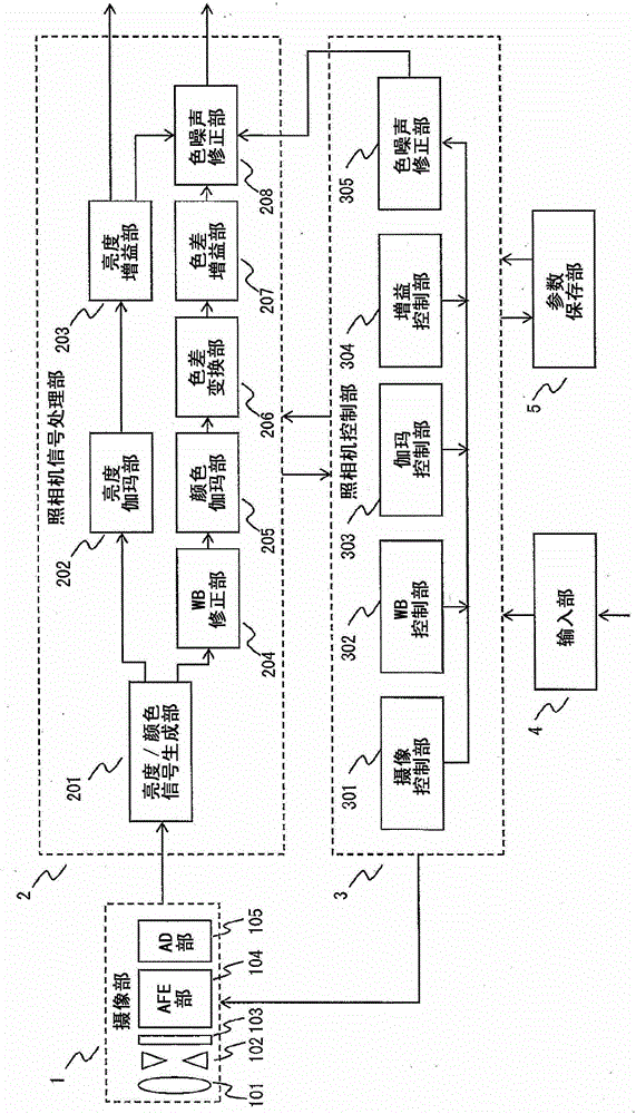
[0036] figure 1 It is a schematic diagram showing the imaging device according to the first embodiment of the present invention. The imaging device according to this embodiment is suitably configured using an imaging unit 1 , a camera signal processing unit 2 , a camera control unit 3 , an input unit 4 , and a parameter storage unit 5 . in addition, figure 1 The arrows between the respective configurations are not necessarily limited thereto, and may be appropriately deleted or changed according to modification examples such as addition, deletion, and replacement of configurations.

[0037] The imaging unit 1 is, for example, suitably constituted by a lens 101, a diaphragm 102, an imaging element 103, an AFE unit 104, and an AD unit 105, and receives images received by an imaging element 103 such as a CCD or a CMOS through the lens 101 and the diaphragm 102. The optical image is subjected to photoelectric conversion, analog signal processing is performed by an AFE unit 104 s...

Embodiment 2

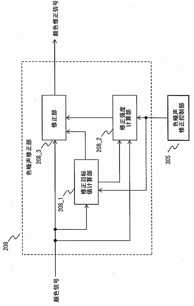
[0060] Figure 6 It is a schematic diagram showing an example of the color noise correction unit of the imaging device according to the second embodiment of the present invention. The other configurations of the imaging device according to the second embodiment are the same as those in the first embodiment, and the same configurations are given the same reference numerals, and their descriptions are appropriately omitted. Here, the explanation will be given mainly with regard to the color noise correcting unit that has a difference. exist Figure 6 In order to illustrate an example of the color noise correction processing by the color noise correction unit 208', only the color noise correction unit 208' and the color noise correction control unit 305 of the imaging device are extracted and described.

[0061] The color noise correction unit 208' is suitably constituted by a correction target value calculation unit 208'_1, a correction strength calculation part 208'_2, a corr...

Embodiment 3

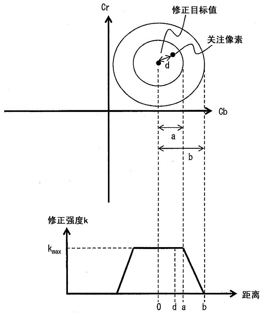
[0068] 9 is a diagram showing an example of color noise correction control processing of the imaging device according to the third embodiment of the present invention. The device configuration is the same as that of the imaging device according to the second embodiment, and description of the details of each configuration will be appropriately omitted. In FIG. 9, as an example of the color noise correction control process linked to the control of the imaging conditions in the camera control unit 3, the color noise correction unit 208' is shown as a configuration in which the characteristic of the correction intensity is changed according to the brightness and the brightness edge. In addition, it is an example in which the color noise correction unit 208 is controlled in conjunction with the control of the gamma characteristic of the luminance gamma of the luminance gamma unit 202 in the camera signal processing unit 2 . In FIG. 9, FIG. 9(a) is a diagram showing the calculation...


PUM


Abstract

The present invention provides an imaging device and an image signal processor. The present invention is configured of an imaging device that has: an imaging unit; a signal processing unit that performs signal processing on an image signal inputted from the imaging unit and outputs a luminance signal and a chrominance signal; a camera controlling unit that controls at least one of photographing conditions of optical conditions and exposure of the photographing unit and a signal processing condition of the signal processing unit; and a color noise correction unit that extracts and corrects a color noise component from the chrominance signal inputted from the signal processing unit. The camera control unit controls the color noise correction unit using information of the photographing conditions. Enhancing the image quality by suitable color noise correction is realized without depending on a subject, a photographing scene, and photographing conditions by determining and correcting a color noise component according to photographing conditions of a camera.

Description

technical field [0001] The present invention relates to an imaging device and an image signal processing device. Background technique [0002] As background technology in this technical field, there is Japanese Patent Laid-Open No. 2007-129524 (Patent Document 1). In this publication, for the purpose of "properly removing color noise based on the gains of the signals of the three primary colors", it is described that "in this digital camera, when performing color noise removal processing, in step S310, the After the white balance gains Rc and Bc, in step S320, the number of times n of filtering processing corresponding to the values ​​of the white balance gains Rc and Bc is read out, and in step S330, the number of times of filtering processing n corresponding to the color difference signals Cr and Cb is read out Corresponding low-pass filtering, thereby carry out smoothing processing.Therefore, by using the white balance gain Rc, Bc to change the value of R, B, even when t...

Claims


Application Information

Patent Timeline
Patent Type & Authority Applications(China)
IPC IPC(8): H04N9/64H04N5/232H04N1/409H04N23/12
CPCH04N9/04H04N9/646H04N9/643H04N9/735
Inventor 广冈慎一郎胜木学盐川淳司野中雄一
Owner HITACHI INFORMATION & CONTROL SOLUTIONS LTD
Learn More