Flexible light emitting semiconductor device having three-dimensional structure

A light-emitting semiconductor, three-dimensional structure technology, applied in the direction of semiconductor devices, semiconductor devices, electric solid devices, etc. of light-emitting elements, can solve the problems of limited use, material deterioration, LES device and package thickness, etc., to achieve enhanced light efficiency, good The effect of thermal management

Inactive Publication Date: 2014-09-03
3M INNOVATIVE PROPERTIES CO
View PDF10 Cites 14 Cited by
  • Summary
  • Abstract
  • Description
  • Claims
  • Application Information

AI Technical Summary

Problems solved by technology

Excessive heat buildup can lead to degradation of materials used in LES devices, such as encapsulants for LESDs
Heat dissipation concerns are greatly increased when LESDs are attached to a flex circuit laminate (which may also include other electronic components)
[0004] Additionally, conventional LES devices and packages tend to be thick, which limits their use in low form factor applications

Method used


Image

  • Flexible light emitting semiconductor device having three-dimensional structure
  • Flexible light emitting semiconductor device having three-dimensional structure
  • Flexible light emitting semiconductor device having three-dimensional structure

Examples


Embodiment Construction

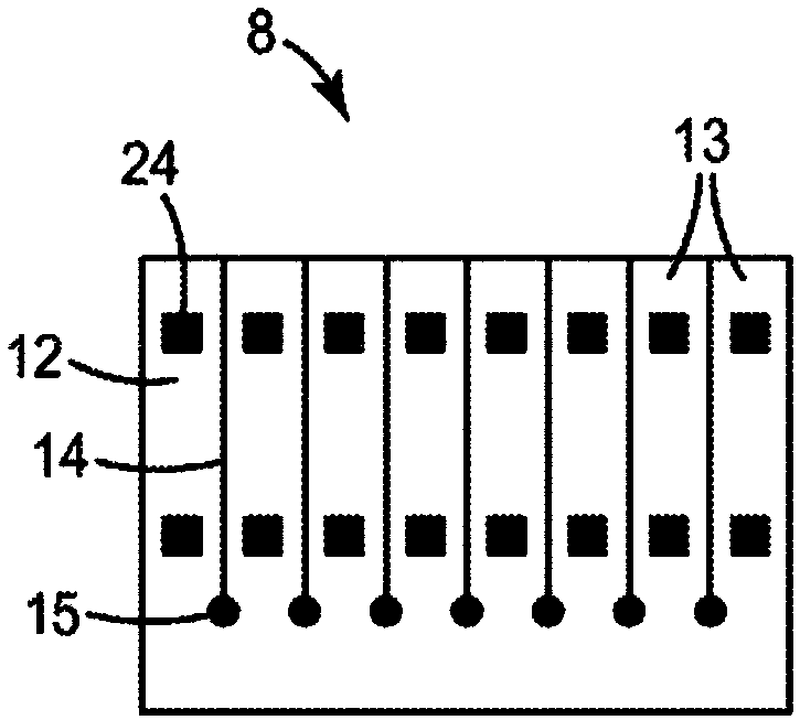
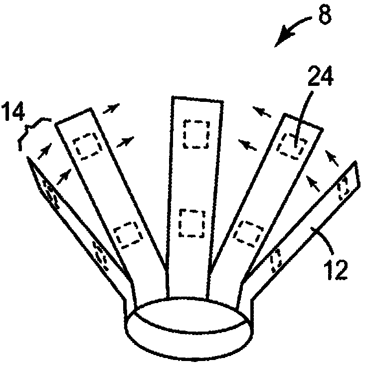
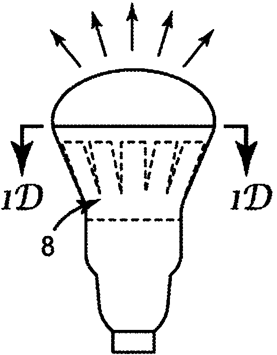
[0023] In the following description, reference is made to the accompanying drawings which form a part hereof, and in which are shown by way of illustration several specific embodiments. In general, similar features use similar reference numbers in various embodiments. These similar features may comprise the same materials, have the same properties and perform the same or similar functions unless otherwise indicated. Additional or optional features described for one embodiment may also be additional or optional features of other embodiments, even if not explicitly stated, where appropriate. It is to be understood that other embodiments may be conceived and practiced without departing from the scope or spirit of the invention. Therefore, the following specific embodiments are not limiting.

[0024] Unless otherwise indicated, all numbers expressing characteristic dimensions, quantities and physical properties used in the specification and claims are to be understood as being m...


PUM


Abstract

Provided is an article comprising a flexible circuit comprising a polymeric dielectric layer having first and second major surfaces, one or both of the first and second major surfaces having a conductive layer thereon, wherein at least one conductive layer comprises an electrical circuit configured to power one or more light emitting semiconductor devices located on the flexible circuit, wherein the flexible circuit is shaped to form a three dimensional structure.

Description

technical field [0001] The present invention relates to flexible light emitting semiconductor devices. Background technique [0002] Conventional light emitting semiconductor (LES) devices (LESDs), including light emitting diodes (LEDs) and laser diodes, and packages containing LESDs have several disadvantages. High power LESDs generate a considerable amount of heat that must be managed. Thermal management deals with issues arising from heat dissipation and thermal stress, which are currently the key factors limiting the performance of LEDs. [0003] In general, LES devices are often susceptible to damage from the buildup of heat generated within the device and, in the case of external lighting applications, from sunlight. Excessive heat buildup can lead to degradation of materials used in LES devices, such as encapsulants for LESDs. Heat dissipation issues are greatly increased when LESDs are attached to a flex circuit laminate (which may also include other electronic co...

Claims


Application Information

Patent Timeline
Patent Type & Authority Applications(China)
IPC IPC(8): F21S2/00H01L33/48H05K3/28F21W107/00
CPCH05K2201/09063F21W2101/00H05K1/189H05K2201/10106H05K1/028F21Y2111/007F21K9/135H05K2201/047F21W2121/00H05K2201/053F21Y2101/02F21V3/00F21V29/004F21K9/00F21V21/14H01L25/0753F21Y2111/001H01L2924/0002F21K9/232F21Y2115/10F21Y2107/00F21Y2107/40F21W2107/00H01L2924/00F21S2/005F21V23/003H01L33/10H01L33/56F21V29/70
Inventor 亚历杭德罗·阿尔德林·阿恰奥伊利·那拉格二世拉维·帕拉尼斯瓦米阿罗基阿拉杰·耶苏多斯朱斯蒂娜·A·穆尼
Owner 3M INNOVATIVE PROPERTIES CO
Why Eureka
Try Eureka