
A dual-wavelength micro-nano structure phase measurement method

A technology of micro-nano structure and phase measurement, which is applied in the direction of measuring devices, instruments, optical devices, etc., and can solve the problem of expanding the range of interferometric measurement

Active Publication Date: 2016-08-17
SOUTH CHINA NORMAL UNIVERSITY
View PDF3 Cites 0 Cited by
  • Summary
  • Abstract
  • Description
  • Claims
  • Application Information

AI Technical Summary

Problems solved by technology

[0003] Aiming at the limitations of various interferometric unwrapping methods at present, the present invention provides an interferometric method that can measure isolated and discontinuous (with mutation) objects, which expands the range of interferometric measurements and breaks through the limitations of traditional phase unwrapping

Method used


Image

  • A dual-wavelength micro-nano structure phase measurement method
  • A dual-wavelength micro-nano structure phase measurement method
  • A dual-wavelength micro-nano structure phase measurement method

Examples


Embodiment 1

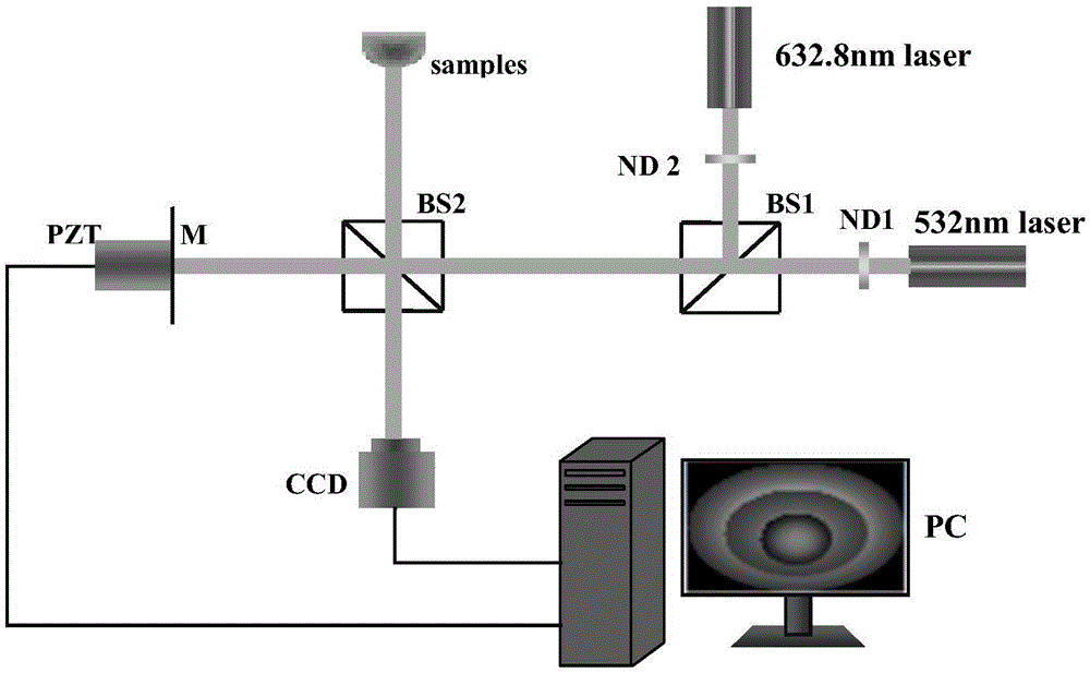
[0058] This example uses the figure 1 The Michelson interference optical path shown is a coaxial phase-shifted interferometric optical path, and the measured object is a commonly used optical element concave mirror. The measurement system includes a light source, a piezoelectric ceramic micro-displacement (PZT), a monochrome image sensor (CCD), and a computer (PC). Among them, the light source is composed of a He-Ne laser with a wavelength of 632.8nm and a solid-state laser with a wavelength of 532nm. The piezoelectric ceramic micro-displacement device is a micro-displacement device of the type 2D020 produced by the 26 Research Institute of the Electronic Industry Group, which is controlled by a computer to form a phase shift subsystem. The image sensor is the MTV-1082CB black and white industrial camera produced by Taiwan Mintong Company, and the image data is stored in the computer through the image acquisition card to form an image acquisition subsystem.

[0059] When imp...

Embodiment 2

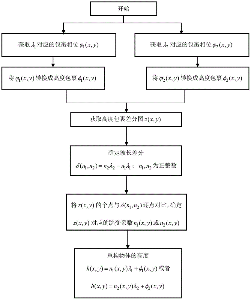
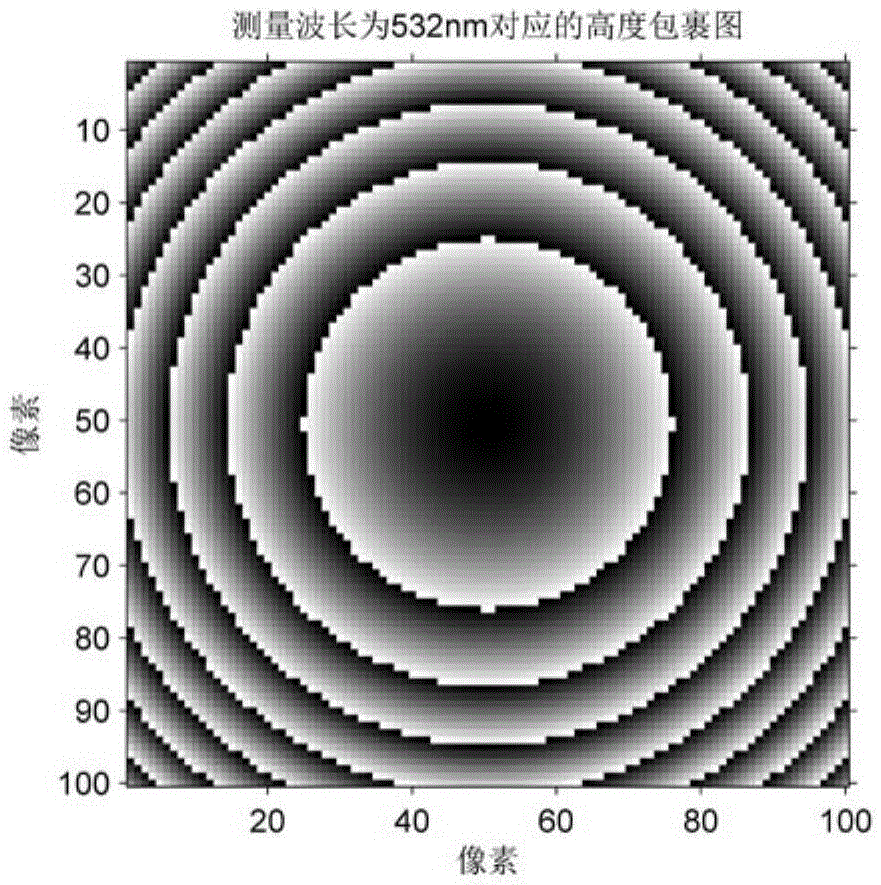
[0068] In order to further prove that this method can be used for phase measurement of isolated discontinuous (with mutation) objects. The present embodiment adopts the method of simulation, applies the method of the present invention to measure the square column of isolated sudden change, as Figure 4a shown. The height of these square pillars is randomly generated within the range of 0-60000 nanometers, that is to say, there are random mutations between 0-60000 nanometers, and there is no correlation between them. The implementation steps are the same as figure 2 The flow chart shown. The height-wrapped grayscale images of these square columns acquired under a light source with a wavelength of 532 nm are shown in Figure 4b As shown, the height-wrapped grayscale image acquired under the light source with a wavelength of 632.8 nm is shown in Figure 4c shown. Subtract the two wavelength height wrapping images to obtain the difference grayscale image of height wrapping a...

Embodiment 3

[0070] The inventive method greatly expands the measuring range of interference precision measurement, according to the inventive method, if there is a greatest common divisor k between the measurement light source wavelengths that adopt, so the measuring range that this method can measure is: (λ 2 / k+1)λ 1 or (λ 1 / k+1)λ 2 . When the wavelength of the measuring light source is 632.8 nm and 532 nm, the greatest common divisor is 56. If the wavelength of 532 nm is used for reconstruction, the range can reach 60648 nm; if the wavelength of 632.8 nm is used for reconstruction, the range can reach 60748.8 nm. In order to prove the range of the method of the present invention, the present embodiment still adopts the method of simulation, and the method of the present invention is used to measure the slope of 0-60648 nanometer linear increase, and there are sudden changes on both sides of the slope, and the slope to be measured is as follows Figure 5a shown. A light source with...


PUM


Abstract

The invention discloses a dual-wavelength micro-nano structure phase measurement method. By using two lasers with different wavelengths as light sources, the phase wrapping diagrams are respectively obtained, and the known fixed relationship between the two wavelengths at the same position (pixel) is used to determine the phase. The phase jump coefficient of the position (pixel) reconstructs the phase of the object. Since the phase information of different positions (pixels) of the object is obtained independently and does not depend on the relationship between adjacent pixels, it can be used to measure the phase information of isolated and non-continuous objects, which can effectively avoid the reason of path dependence in the unwrapping algorithm The phenomenon of error accumulation and propagation can be used not only for continuous smooth objects, but also for phase measurement of isolated discontinuous (with mutation) objects. At the same time, the method of the invention greatly expands the range of effective measurement of mutation objects. The invention has the advantages of simple measuring method, large measuring range, high precision, real-time, efficient and quick measurement.

Description

technical field [0001] The invention relates to an interferometric measurement method applied to the appearance of a micro-nano structure object, belonging to the field of photoelectric detection technology. Background technique [0002] The interferometry method is a common method to obtain the micro-nano structure of the object morphology (phase). Through the interferogram formed between the object light and the reference light carrying the phase information of the object, the three-dimensional information of the object can be obtained by using the phase extraction algorithm. Thanks to the use of laser light as a metrology means, nanometer-accurate measurements can be achieved. The commonly used interferometry method, combined with the use of phase-shift technology, can achieve a measurement accuracy of one hundredth of a wavelength. However, since the obtained phase is expressed by the arctangent function, the phase values ​​obtained by this method are distributed in the...

Claims


Application Information

Patent Timeline
Patent Type & Authority Patents(China)
IPC IPC(8): G01B11/24
Inventor 刘胜德吕晓旭钟丽云
Owner SOUTH CHINA NORMAL UNIVERSITY
Learn More