
Touch display panel and touch display device

A touch display panel and touch display device technology, applied in optics, instruments, electrical digital data processing, etc., can solve the problems of scratches on the color resist surface, affecting the size of the frame, prone to electrostatic discharge, etc., to increase the production quality rate effect

Active Publication Date: 2014-09-10
ACER INC
View PDF4 Cites 14 Cited by
  • Summary
  • Abstract
  • Description
  • Claims
  • Application Information

AI Technical Summary

Problems solved by technology

[0003] Therefore, on the panel manufacturing side, an integrated (on-cell) product has been developed, in which the indium tin oxide layer is fabricated on the other side of the color filter (Color Filter), that is, the color resist and the Indium tin oxide layer, but because the glass needs to be turned over during the manufacturing process, not only is it prone to the risk of Electrostatic Discharge (ESD), it is also easy to cause scratches on the color resistance surface, and because the metal connecting the indium tin oxide layer The wires are routed on the color filter, and the joint space of the flexible printed circuit (FPC) must be designed on the color filter, which also affects the size of the frame

Method used


Image

  • Touch display panel and touch display device
  • Touch display panel and touch display device
  • Touch display panel and touch display device

Examples


Embodiment Construction

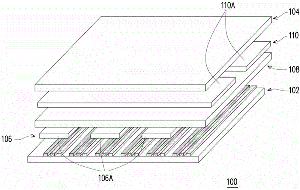
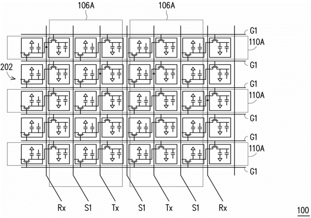
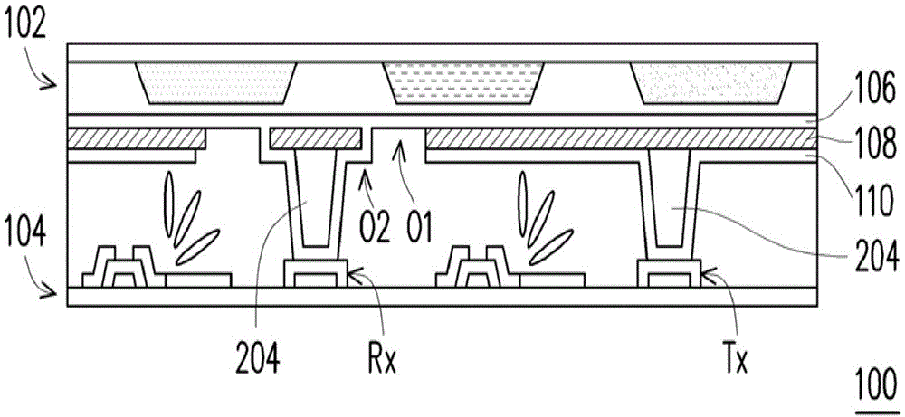
[0049] figure 1 It is a schematic diagram of a touch display panel according to an embodiment of the present invention, please refer to figure 1 . The touch display panel 100 includes a color filter substrate 102 , an active element array substrate 104 , a first transparent conductive layer 106 , an insulating layer 108 and a second transparent conductive layer 110 . Wherein the color filter substrate 102 has red, green and blue (RGB) color resists, and the first transparent conductive layer 106 and the second transparent conductive layer 110 can be, for example, indium tin oxide layers. The first transparent conductive layer 106 , the insulating layer 108 and the second transparent conductive layer 110 are located between the color filter substrate 102 and the active element array substrate 104 , and are disposed on the same side as the RGB color resist. The first transparent conductive layer 106 is disposed on the color filter substrate 102. In this embodiment, the first t...


PUM


Abstract

The invention provides a touch display panel and a touch display device. A first transparent conductive layer, an insulating layer and a second transparent conductive layer are configured on the same side of a color filter substrate, and a touch scanning line and a touch sensing line are configured on one side of an active element array substrate to improve the manufacture yield of the touch display panel.

Description

technical field [0001] The present invention relates to a touch display panel and a touch display device, and in particular to a touch display panel and a touch display device capable of improving yield. Background technique [0002] In the current design of capacitive touch panels, there are mainly designs in which the indium tin oxide (ITO) layer is made on the glass and then laminated on the strengthened glass, which is called GG (Glass Glass). The design that is made on a polyethylene terephthalate (PET) film and then laminated on the strengthened glass is called GFF (Glass Film Film), but the above design will make the touch And the thickness of the display module is thicker, the bonding process will also increase the cost and reduce the yield rate, and the metal wiring connected to the ITO will also increase the thickness of the border. To solve the above problems, a monolithic glass type has been developed. (One Glass Solution, OGS) method, the indium tin oxide layer...

Claims


Application Information

Patent Timeline
IPC IPC(8): G06F3/041G06F3/044G02F1/1362G02F1/1333
Inventor 郭峻廷
Owner ACER INC
Features
  • Generate Ideas
  • Intellectual Property
  • Life Sciences
  • Materials
  • Tech Scout
  • Unparalleled Data Quality
  • Higher Quality Content
  • 60% Fewer Hallucinations
Learn More