Array substrate preparation method, array substrate and display device
An array substrate and graphics technology, applied in semiconductor/solid-state device manufacturing, electrical components, electrical solid-state devices, etc., can solve problems such as low efficiency, high production cost, and greater impact on production capacity, and achieve simplified manufacturing processes, increased production capacity, The effect of reducing production costs
- Summary
- Abstract
- Description
- Claims
- Application Information
AI Technical Summary
Problems solved by technology
Method used
Image

Examples
Embodiment 1
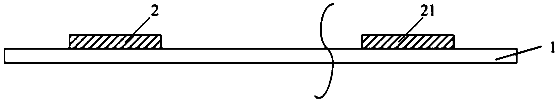
[0052] A preparation method for an array substrate, comprising the step of forming a thin film transistor, a pixel electrode, a common electrode line, and a gate line and a data line electrically connected to the thin film transistor, and forming the thin film transistor includes forming a gate electrode, a gate insulating layer, a semiconductor layer 1. A step of etching the pattern of the barrier layer, the source electrode and the drain electrode, the gate electrode and the common electrode line are formed on the same layer. In the preparation method of the array substrate of this embodiment, the gate insulating film and the semiconductor film are sequentially formed, and a pattern including the semiconductor layer is formed through a patterning process; The pattern of the etch barrier layer.
[0053] Wherein, forming a pattern comprising a gate insulating layer and an etching barrier layer through a patterning process includes: forming a pattern comprising a gate insulatin...
Embodiment 2
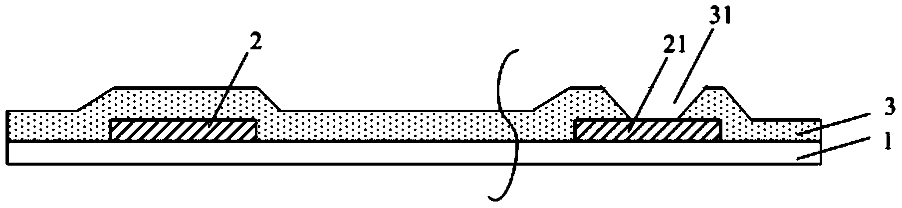
[0071] This embodiment provides a method for preparing an array substrate, including the steps of forming a thin film transistor, a pixel electrode, a common electrode line, and a gate line and a data line electrically connected to the thin film transistor. Layer, semiconductor layer, etch stop layer, patterning of source and drain, gate and common electrode lines are formed in the same layer. In the manufacturing method of the array substrate of this embodiment, the semiconductor thin film and the etch stop film are sequentially formed, and a pattern including the semiconductor layer and the etch stop layer is formed through one patterning process.
[0072] Wherein, forming the pattern including the semiconductor layer and the etching barrier layer through one patterning process includes: forming the pattern including the semiconductor layer and the etching barrier layer with the same projected area through one patterning process.
[0073] Specifically, before sequentially fo...
Embodiment 3
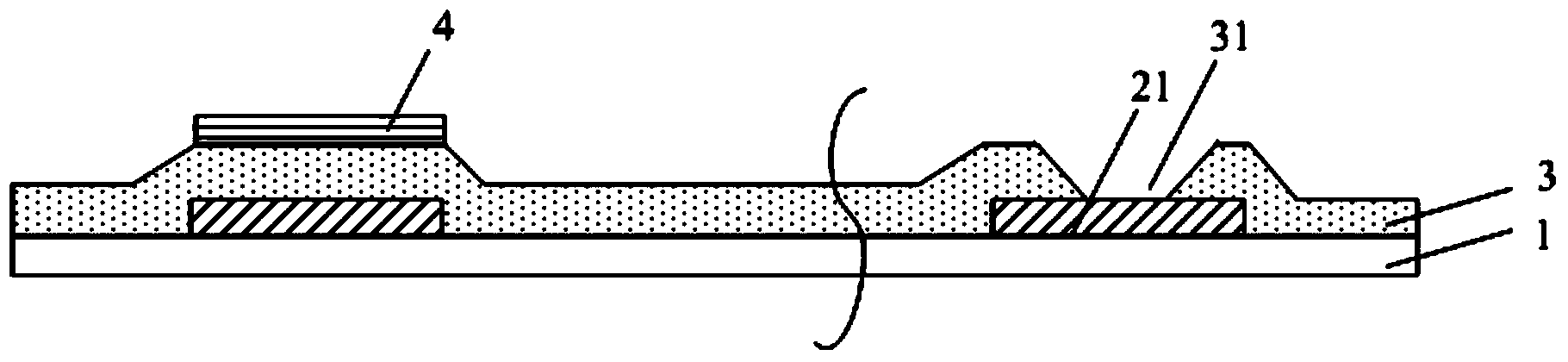
[0096] This embodiment provides a method for preparing an array substrate, including the steps of forming a thin film transistor, a pixel electrode, a common electrode line, and a gate line and a data line electrically connected to the thin film transistor. Layer, semiconductor layer, etch stop layer, patterning of source and drain, gate and common electrode lines are formed in the same layer. In the manufacturing method of the array substrate of this embodiment, the etching stopper film and the transparent electrode film are sequentially formed, and a pattern including the etch stopper layer and the pixel electrode is formed through one patterning process.
[0097] Wherein, forming a pattern comprising an etching barrier layer and a pixel electrode through a patterning process includes: forming a pattern comprising an etching barrier layer and a pixel electrode having the same projected area through a patterning process, and forming a pattern comprising an etching barrier laye...
PUM
 Abstract
Description
Claims
Application Information
 - R&D
- Intellectual Property
- Life Sciences
- Materials
- Tech Scout
- Unparalleled Data Quality
- Higher Quality Content
- 60% Fewer Hallucinations
Browse by: Latest US Patents, China's latest patents, Technical Efficacy Thesaurus, Application Domain, Technology Topic, Popular Technical Reports.
© 2025 PatSnap. All rights reserved.Legal|Privacy policy|Modern Slavery Act Transparency Statement|Sitemap|About US| Contact US: help@patsnap.com