Base plate packaging method

A packaging method and substrate technology, applied to semiconductor devices, electrical components, circuits, etc., can solve the problems of complex manufacturing process, expensive equipment, poor ability to prevent water vapor and oxygen, etc., and achieve extended service life, strong operability, and packaging The effect of simple method

Inactive Publication Date: 2014-09-10
TCL CHINA STAR OPTOELECTRONICS TECH CO LTD
View PDF5 Cites 14 Cited by
  • Summary
  • Abstract
  • Description
  • Claims
  • Application Information

AI Technical Summary

Problems solved by technology

Since the OLED device 400 disposed on the TFT substrate 300 is very sensitive to water vapor and oxygen, but the existing UV encapsulation method has poor ability to prevent water vapor and oxygen, so it is usually necessary to set a desiccant to reduce the penetration of UV glue. The water vapor in the internal sealing area prolongs the service life of the OLED device. The problem caused by this is that the existing UV packaging method is only suitable for the bottom-emitting OLED device structure
The Frit package has a good water blocking effect, but the manufacturing process is complicated and the equipment is expensive.

Method used


Image

  • Base plate packaging method
  • Base plate packaging method
  • Base plate packaging method

Examples


Embodiment Construction

[0041] In order to further illustrate the technical means adopted by the present invention and its effects, the following describes in detail in conjunction with preferred embodiments of the present invention and accompanying drawings.

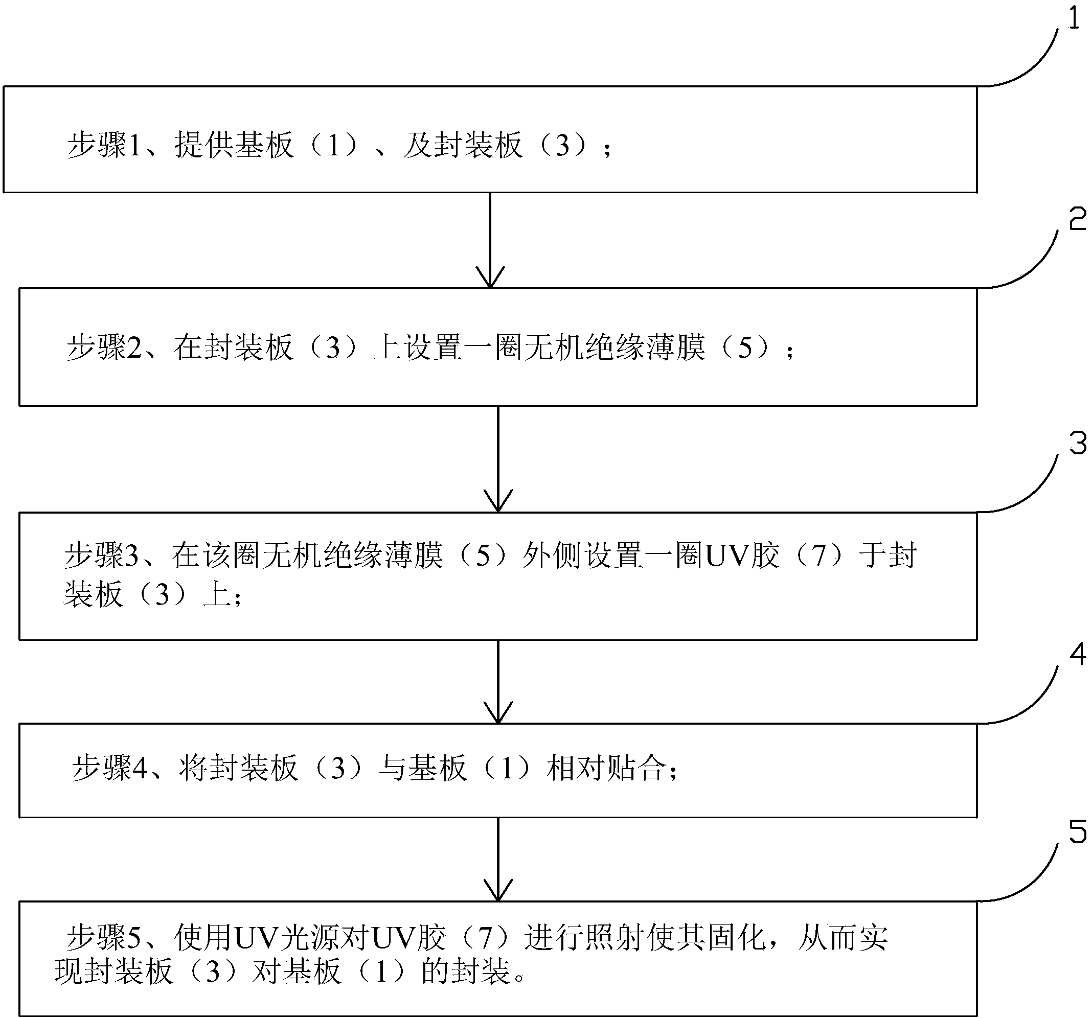
[0042] see Figure 3 to Figure 10 , the present invention provides a substrate packaging method, comprising the following steps:

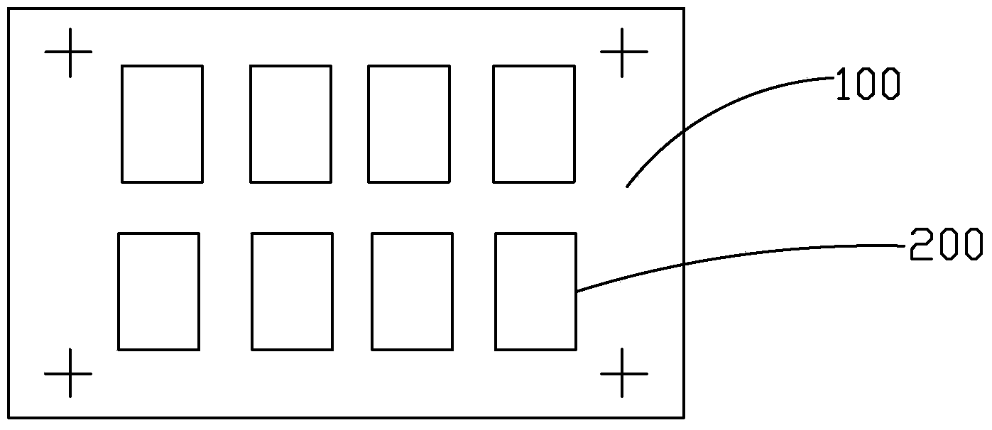
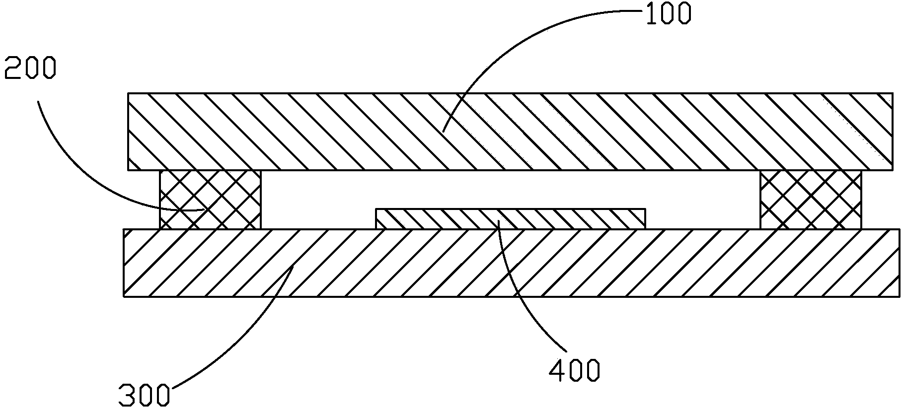
[0043] Step 1, providing a substrate 1 and a packaging board 3;

[0044] Step 2, setting a circle of inorganic insulating film 5 on the packaging board 3;

[0045] Step 3, arrange a circle of UV glue 7 on the packaging board 3 outside the circle of inorganic insulating film 5;

[0046] Step 4, relatively attaching the packaging board 3 to the substrate 1;

[0047] Step 5, using a UV light source to irradiate the UV glue 7 to cure it, so as to realize the packaging of the substrate 1 by the packaging board 3 .

[0048] Specifically, the substrate 1 in the step 1 is a TFT substrate, and the packaging plate 3 is a...


PUM


Abstract

The invention provides a base plate packaging method which includes the following steps: 1 providing a base plate (1) and a packaging plate (3); 2 arranging a ring of inorganic insulation film (5) is arranged on the packaging plate (3); 3 arranging a ring of ultraviolet glue (7) on the outside of the inorganic insulation film (5) on the packaging plate (3); 4 bonding the packaging plate (3) and the base plate (1) relatively; 5 utilizing a UV light source to irradiate the UV glue (7) to enable the UV glue to be solidified to achieve package of the base plate (1) by the packaging plate (3). By means of the packaging method, the packaging effect is improved, the steam and oxygen blocking capability is improved, the service life of an organic light emitting diode (OLED) device is prolonged, and the method is simple, feasible and good in operability.

Description

technical field [0001] The present invention relates to the field of display technology, in particular to a substrate packaging method. Background technique [0002] In the field of display technology, flat panel display technologies such as Liquid Crystal Display (LCD) and Organic Light Emitting Diode (OLED) have gradually replaced CRT displays. Planar light source technology is a new type of light source, and its technology research and development is close to the market-oriented mass production level. In flat panel display and planar light source technology, the bonding of two pieces of flat glass is a very important technology, and its packaging effect will directly affect the performance of the device. [0003] Ultraviolet (UV) curing technology is the earliest and most commonly used technology for LCD / OLED packaging. It has the following characteristics: no solvent or a small amount of solvent is used, which reduces the pollution of the solvent to the environment; it ...

Claims


Application Information

Patent Timeline
Patent Type & Authority Applications(China)
IPC IPC(8): H01L51/56
CPCH10K50/8426H10K71/00H10K71/50H10K59/00H10K71/231
Inventor 刘亚伟
Owner TCL CHINA STAR OPTOELECTRONICS TECH CO LTD
Why Eureka
Try Eureka