Encapsulation structure and method of micro electro mechanical system device

A micro-electro-mechanical system and packaging structure technology, which is applied in the direction of micro-electronic micro-structure devices, micro-structure technology, electric solid-state devices, etc., can solve the problems of high process difficulty, high cost, and low air-tightness, and achieve simple manufacturing process and high production efficiency. Low cost and good air tightness

Inactive Publication Date: 2017-08-18
SHANGHAI HUAHONG GRACE SEMICON MFG CORP
View PDF9 Cites 3 Cited by
  • Summary
  • Abstract
  • Description
  • Claims
  • Application Information

AI Technical Summary

Problems solved by technology

[0003] Since most MEMS devices have airtightness requirements, such as a microbolometer (Micro-bolometer) in the infrared sensor, in the prior art, the packaging method of the MEMS sensor usually adopts a cap that forms a closed space, Through-silicon vias are formed on the cap to realize the electrical connection of MEMS and meet airtightness requirements, but the traditional packaging method requires additional processing of the cap, which has problems such as high process difficulty, low airtightness and high cost

Method used


Image

  • Encapsulation structure and method of micro electro mechanical system device
  • Encapsulation structure and method of micro electro mechanical system device
  • Encapsulation structure and method of micro electro mechanical system device

Examples


Embodiment Construction

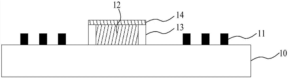
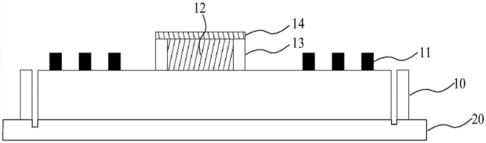
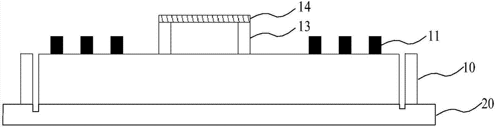
[0037] Such as Figure 1 to Figure 4 As shown, it is a structural diagram corresponding to each step in an infrared sensor packaging method well known to the inventor. First, if figure 1 As shown, a first substrate 10 is provided, which includes a corresponding circuit structure, and then a number of contact holes 11 are formed on the first plane of the first substrate 10 for realizing the circuit structure. External electrical connection; In addition, a sacrificial layer 12 is formed on the first plane of the first substrate 10, and the sacrificial layer 12 can be commonly used materials such as silicon oxide, amorphous silicon or photosensitive polyimide; A microbridge structure 13 is formed on the sidewall of the sacrificial layer 12, and a photosensitive material layer 14 is formed, and the photosensitive material layer covers the sacrificial layer 12 and the microbridge structure 13. The above structures can be collectively referred to as a chip to be packaged. circle; ...


PUM


Abstract

The invention discloses an encapsulation structure and method of a micro electro mechanical system device. The encapsulation structure of the micro electro mechanical system device comprises a first wafer and a second wafer; the first wafer is provided with a first central region and a first marginal region surrounding the first central region; the second wafer is provided with a second central region and a second marginal region surrounding the second central region; a first closed space is formed between the first central region and the second central region by correspondingly binding the first binding structure of the first marginal region and the second binding structure of the second marginal region together, namely, the micro electro mechanical system device in the first wafer is located in the closed space; the encapsulation structure of the formed micro electro mechanical system device is excellent in sealing; and the manufacturing procedure of the second wafer is simple and easy and free from additional processing. Therefore, the encapsulation structure of the micro electro mechanical system device disclosed by the invention is good in air tightness, simple and easy in encapsulation method, and low in production cost.

Description

technical field [0001] The invention relates to the technical field of semiconductor packaging, in particular to a packaging structure and method for micro-electromechanical system devices. Background technique [0002] Micro-Electro-Mechanical System (MEMS) sensor is a new type of sensor manufactured by microelectronics and micromachining technology. Compared with traditional sensors, it has the characteristics of small size, light weight, low cost, low power consumption, high reliability, suitable for mass production, easy integration and intelligentization. [0003] Since most MEMS devices have airtightness requirements, such as a microbolometer (Micro-bolometer) in the infrared sensor, in the prior art, the packaging method of the MEMS sensor usually adopts a cap that forms a closed space, Through-silicon vias are formed on the cap to realize the electrical connection of MEMS and meet airtightness requirements, but the traditional packaging method requires additional pr...

Claims


Application Information

Patent Timeline
Patent Type & Authority Applications(China)
IPC IPC(8): B81B7/00B81C1/00
CPCB81B7/0035B81C1/00277B81B2201/0207B81C2203/0118B81C2203/019B81B7/007B81C1/00317B81B2201/0292H01L31/0203H01L2224/48091H01L2924/00014B81B7/0067B81C1/00134
Inventor 刘玮荪
Owner SHANGHAI HUAHONG GRACE SEMICON MFG CORP
Why Eureka
Try Eureka