Organic light emitting diode device and preparation method thereof

An electroluminescent device, organic technology, applied in the direction of electric solid state device, semiconductor/solid state device manufacturing, electrical components, etc.

Inactive Publication Date: 2015-04-15
OCEANS KING LIGHTING SCI&TECH CO LTD +2
View PDF0 Cites 3 Cited by
  • Summary
  • Abstract
  • Description
  • Claims
  • Application Information

AI Technical Summary

Problems solved by technology

The method of the invention is especially suitable fo...

Method used


Image

  • Organic light emitting diode device and preparation method thereof
  • Organic light emitting diode device and preparation method thereof
  • Organic light emitting diode device and preparation method thereof

Examples


Embodiment 1

[0062] A method for preparing an organic electroluminescent device, comprising the following steps:

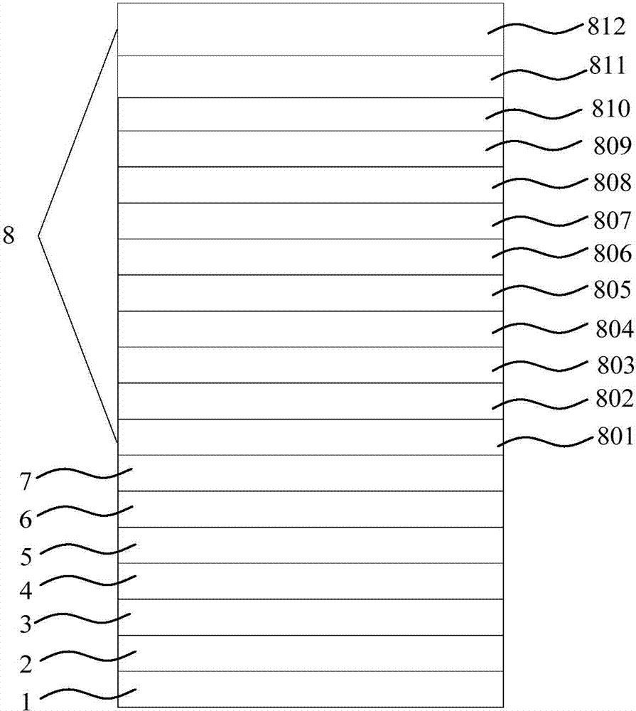
[0063] (1) Pre-treatment of ITO conductive glass substrate 1: put ITO conductive glass substrate 1 into acetone, ethanol, deionized water, and ethanol in sequence, ultrasonically clean them for 5 minutes, then blow dry with nitrogen, and dry them in an oven for later use; The cleaned ITO glass substrate 1 is subjected to surface activation treatment to increase the oxygen content of the conductive surface layer and improve the work function of the conductive layer surface; the thickness of the ITO glass substrate 1 is 100nm;

[0064] Hole injection layer 2: Evaporate MoO on the ITO conductive glass substrate 1 3 Hybrid material obtained by doping NPB, MoO 3 The doping mass fraction in NPB is 30%, and the evaporation is carried out by high-vacuum coating equipment, and the vacuum degree during evaporation is 1×10 -5 Pa, the evaporation rate is A hole injection layer 2 is ob...

Embodiment 2

[0082] A method for preparing an organic electroluminescent device, comprising the following steps:

[0083] Step (1) is the same as embodiment 1;

[0084] (2) Place the organic electroluminescent device sample in a vacuum coating machine, and prepare a mixed barrier layer by vacuum evaporation on the organic electroluminescent device sample. The material of the mixed barrier layer is ZnPc, NPB, CeF 2 and V 2 o 5 Formed hybrid materials, ZnPc, CeF 2 and V 2 o 5 The mole fractions of the mixed materials are 40%, 15% and 10%, respectively, and the evaporation vacuum is 5×10 -5 Pa, the evaporation rate of ZnPc is The thickness of the mixed barrier layer is 150nm;

[0085] (3) The inorganic barrier layer was prepared by atomic layer deposition on the mixed barrier layer, and the material of the inorganic barrier layer was ZrO 2 ;

[0086] A preparation cycle for preparing an inorganic barrier layer is:

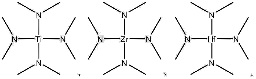
[0087] (a) [Zr(N(CH 3 ) 2 ) 4 ] is injected into the deposition...

Embodiment 3

[0095] A method for preparing an organic electroluminescent device, comprising the following steps:

[0096] Step (1) is the same as embodiment 1;

[0097] (2) Place the organic electroluminescent device sample in a vacuum coating machine, and prepare a mixed barrier layer by vacuum evaporation on the organic electroluminescent device sample. The material of the mixed barrier layer is FePc, Alq3, MgF 2 and WO 3 Formed hybrid materials, FePc, Alq3 and WO 3 The mole fractions of the mixed materials are 60%, 10% and 20% respectively, and the evaporation vacuum is 5×10 -5 Pa, the evaporation rate of FePc is The thickness of the mixed barrier layer is 100nm;

[0098] (3) The inorganic barrier layer was prepared by atomic layer deposition on the mixed barrier layer, and the material of the inorganic barrier layer was HfO 2 ;

[0099] A preparation cycle for preparing an inorganic barrier layer is:

[0100] (a) [Hf(N(CH 3 ) 2 ) 4 ] is injected into the deposition chamber of ...


PUM

PropertyMeasurementUnit
Thicknessaaaaaaaaaa
Thicknessaaaaaaaaaa
Thicknessaaaaaaaaaa

Abstract

The invention provides an organic light emitting diode device. The organic light emitting diode device includes an anode electric conduction substrate, a hole injection layer, a hole transport layer, a light-emitting layer, an electron transport layer, an electron injection layer, a cathode layer and an encapsulation layer which are stacked to one another sequentially; the anode electric conduction substrate and the encapsulation layer form a closed space; the hole injection layer, the hole transport layer, the light-emitting layer, the electron transport layer, the electron injection layer and the cathode layer are accommodated in the closed space; and the encapsulation layer includes hybrid barrier layers and inorganic barrier layers which are stacked sequentially, wherein the hybrid barrier layers are made of a mixture of phthalocyanine, fluoride, an organic material and an oxide, and the inorganic barrier layers are made of titanium dioxide, zirconium dioxide or hafnium dioxide. The method provided by the invention is especially suitable for the encapsulation of flexible organic light emitting diode devices.

Description

technical field [0001] The invention relates to the related field of electronic devices, in particular to an organic electroluminescent device and a preparation method thereof. Background technique [0002] Organic electroluminescent device (OLED) is a current-mode semiconductor light-emitting device based on organic materials. Its typical structure is to prepare an organic luminescent material with a thickness of tens of nanometers on the ITO glass as a light-emitting layer, and a metal electrode with a low work function is placed above the light-emitting layer. When a voltage is applied to the electrodes, the light-emitting layer produces light radiation. [0003] OLED devices have the advantages of active luminescence, high luminous efficiency, low power consumption, lightness, thinness, and no viewing angle restrictions. They are considered by industry insiders to be the new generation of devices that are most likely to occupy a dominant position in the future lighting ...

Claims


Application Information

Patent Timeline
IPC IPC(8): H01L51/52H01L51/54H01L51/56
CPCH10K71/166H10K85/311H10K50/8445
Inventor 周明杰钟铁涛王平张振华
Owner OCEANS KING LIGHTING SCI&TECH CO LTD
Why Eureka
Try Eureka