Organic light emitting diode device and preparation method thereof

An electroluminescent device and luminescent technology, which is applied in the direction of electric solid-state devices, semiconductor/solid-state device manufacturing, electrical components, etc., can solve the problems of short life, affect the life of the device, increase the weight of the device, etc., and prevent the erosion of water and oxygen , Good shape retention and high compactness

Inactive Publication Date: 2015-04-15
OCEANS KING LIGHTING SCI&TECH CO LTD +2
View PDF0 Cites 3 Cited by
  • Summary
  • Abstract
  • Description
  • Claims
  • Application Information

AI Technical Summary

Problems solved by technology

[0004] Flexible products are the development trend of organic electroluminescent devices, but at present, the lifespan is generally short, so the quality of the packaging directly affects the lifespan of the device
In the traditional technology, a glass cover or a metal cover is used for encapsulation, and its edge is sealed with ultraviolet polymer resin, but the glass cover or metal cover used in this method is often large in size, which increases the weight of the device, and this method cannot be applied to flexible devices. Encapsulation of Organic Electroluminescent Devices

Method used


Image

  • Organic light emitting diode device and preparation method thereof
  • Organic light emitting diode device and preparation method thereof
  • Organic light emitting diode device and preparation method thereof

Examples


Embodiment 1

[0062] A method for preparing an organic electroluminescent device, comprising the following steps:

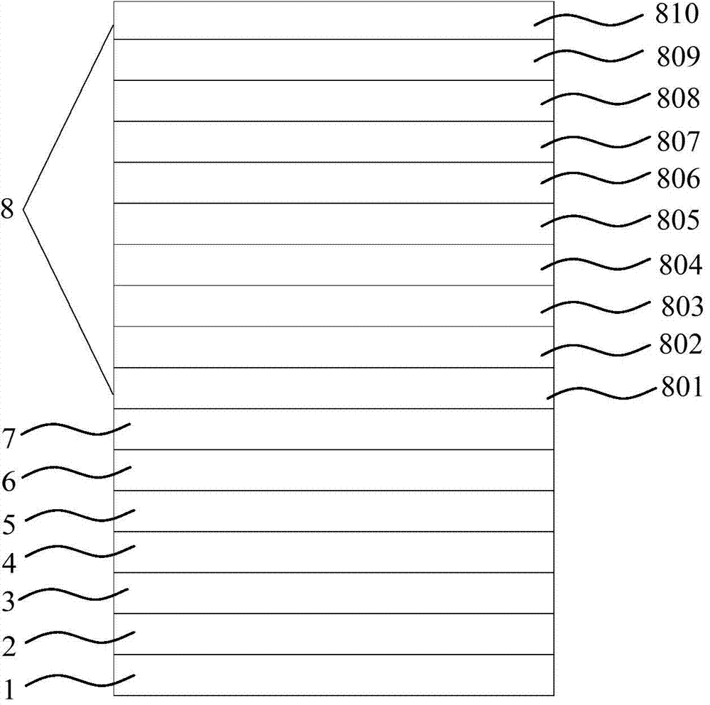
[0063] (1) Pre-treatment of ITO conductive glass substrate 1: put ITO conductive glass substrate 1 into acetone, ethanol, deionized water, and ethanol in sequence, ultrasonically clean them for 5 minutes, then blow dry with nitrogen, and dry them in an oven for later use; The cleaned ITO glass substrate 1 is subjected to surface activation treatment to increase the oxygen content of the conductive surface layer and improve the work function of the conductive layer surface; the thickness of the ITO glass substrate 1 is 100nm;

[0064] Hole injection layer 2: Evaporate MoO on the ITO conductive glass substrate 1 3 The mixed material obtained by doping NPB, the doping mass fraction of MoO3 in NPB is 25%, and the evaporation is carried out by high vacuum coating equipment, and the vacuum degree during evaporation is 3×10 -5 Pa, the evaporation rate is A hole injection layer 2 i...

Embodiment 2

[0082] A method for preparing an organic electroluminescent device, comprising the following steps:

[0083] Step (1) is the same as embodiment 1;

[0084] (2) Place the organic electroluminescent device sample in a plasma-enhanced chemical vapor deposition chamber, the silicon source and carbon source are methyl silane, and the nitrogen source is NH 3 , while passing into H 2 , the flow of methyl silane is 8 sccm, the flow of ammonia is 24 times of the flow of methyl silane, H 2 The flow rate is 205sccm, and the thickness of the silicon nitride carbide layer is 140nm;

[0085] (3) On the silicon carbonitride layer, an inorganic barrier layer was prepared by atomic layer deposition, and the material of the inorganic barrier layer was Al 2 o 3 ;

[0086] A preparation cycle for preparing an inorganic barrier layer is:

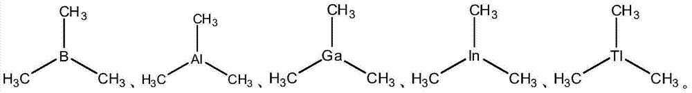
[0087] (a) Al(CH 3 ) 3 The nitrogen gas is injected into the deposition chamber of the atomic layer deposition system and deposited on the silicon carbo...

Embodiment 3

[0095] A method for preparing an organic electroluminescent device, comprising the following steps:

[0096] Step (1) is the same as embodiment 1;

[0097] (2) Place the organic electroluminescent device sample in a plasma-enhanced chemical vapor deposition chamber, the silicon source and carbon source are methyl silane, and the nitrogen source is NH 3 , while passing into H 2 , the flow of methyl silane is 6 sccm, the flow of ammonia is 21 times of the flow of methyl silane, H 2 The flow rate is 210sccm, and the thickness of the silicon carbide layer is 140nm;

[0098] (3) The inorganic barrier layer was prepared by atomic layer deposition on the silicon carbonitride layer, and the material of the inorganic barrier layer was Ga 2 o 3 ;

[0099] A preparation cycle for preparing an inorganic barrier layer is:

[0100] (a) Ga(CH 3 ) 3 The nitrogen gas is injected into the deposition chamber of the atomic layer deposition system and deposited on the silicon carbonitride ...


PUM


Abstract

The invention provides an organic light emitting diode device. The organic light emitting diode device includes an anode electric conduction substrate, a hole injection layer, a hole transport layer, a light-emitting layer, an electron transport layer, an electron injection layer, a cathode layer and an encapsulation layer which are stacked to one another sequentially; the anode electric conduction substrate and the encapsulation layer form a closed space; the hole injection layer, the hole transport layer, the light-emitting layer, the electron transport layer, the electron injection layer and the cathode layer are accommodated in the closed space; and the encapsulation layer includes silicon carbonitride layers and inorganic barrier layers which are stacked sequentially, wherein the inorganic barrier layers are made of boric oxide, aluminum oxide, gallium oxide, indium oxide or thallium oxide. The method provided by the invention is especially suitable for the encapsulation of flexible organic light emitting diode devices.

Description

technical field [0001] The invention relates to the related field of electronic devices, in particular to an organic electroluminescent device and a preparation method thereof. Background technique [0002] Organic electroluminescent device (OLED) is a current-mode semiconductor light-emitting device based on organic materials. Its typical structure is to prepare an organic luminescent material with a thickness of tens of nanometers on the ITO glass as a light-emitting layer, and a metal electrode with a low work function is placed above the light-emitting layer. When a voltage is applied to the electrodes, the light-emitting layer produces light radiation. [0003] OLED devices have the advantages of active luminescence, high luminous efficiency, low power consumption, lightness, thinness, and no viewing angle restrictions. They are considered by industry insiders to be the new generation of devices that are most likely to occupy a dominant position in the future lighting ...

Claims


Application Information

Patent Timeline
Patent Type & Authority Applications(China)
IPC IPC(8): H01L51/50H01L51/52H01L51/54H01L51/56
CPCH10K50/8445H10K50/844H10K71/00
Inventor 周明杰钟铁涛王平张振华
Owner OCEANS KING LIGHTING SCI&TECH CO LTD
Why Eureka
Try Eureka