Micro-nano structure sidewall surface imaging device based on atomic force microscope (AFM) and imaging method thereof

An atomic force microscope and micro-nano structure technology, which can be used in measurement devices, scanning probe microscopy, instruments, etc. Usability and operability effects

Inactive Publication Date: 2014-09-24
HARBIN INST OF TECH
View PDF4 Cites 19 Cited by
  • Summary
  • Abstract
  • Description
  • Claims
  • Application Information

AI Technical Summary

Problems solved by technology

[0003] The purpose of the present invention is to solve the problem that the traditional atomic force microscope (AFM) is difficult to scan and image the side wall surface of the micro-nano structure, and provide a micro-nano structure side wall surface imaging device based on the atomic force microscope and an imaging method for the device

Method used


Image

  • Micro-nano structure sidewall surface imaging device based on atomic force microscope (AFM) and imaging method thereof
  • Micro-nano structure sidewall surface imaging device based on atomic force microscope (AFM) and imaging method thereof
  • Micro-nano structure sidewall surface imaging device based on atomic force microscope (AFM) and imaging method thereof

Examples


specific Embodiment approach 1

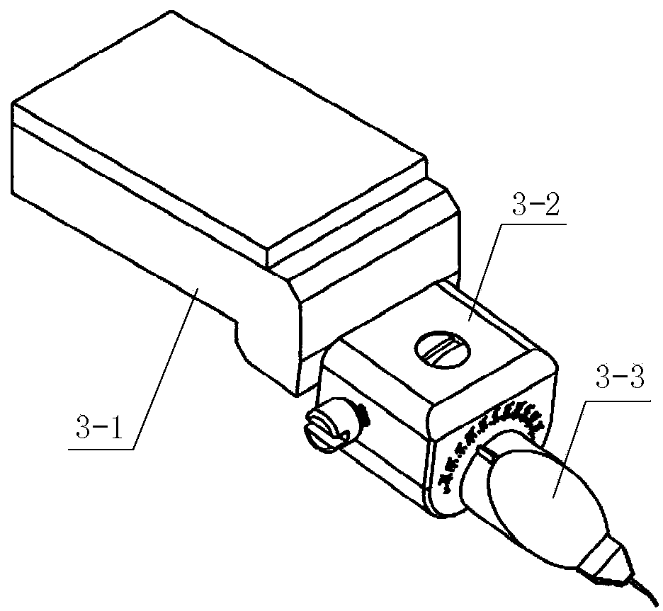
[0033] Specific implementation mode one: combine Figure 1 to Figure 5 Describe this embodiment mode, the micro-nano structure side wall surface imaging device based on the atomic force microscope described in this embodiment mode includes an atomic force microscope and a probe frame 3, and the probe frame 3 includes a base 3-1 and a rotating arm 3- 3. The rotating arm 3-3 is arranged on the base 3-1, and the rotating arm 3-3 can rotate around its central axis. The base 3-1 is used to fix the probe frame 3 on the probe hand of the atomic force microscope. 4, the probe of the atomic force microscope is fixed on the rotating arm 3-3 of the probe holder 3, and the cross section of the probe is circular or elliptical.

[0034] The micro-nano structure sidewall surface imaging device based on the atomic force microscope described in this embodiment adds a probe holder 3 on the basis of the original atomic force microscope, such as figure 1 As shown, the probe frame 3 is located betw...

specific Embodiment approach 2

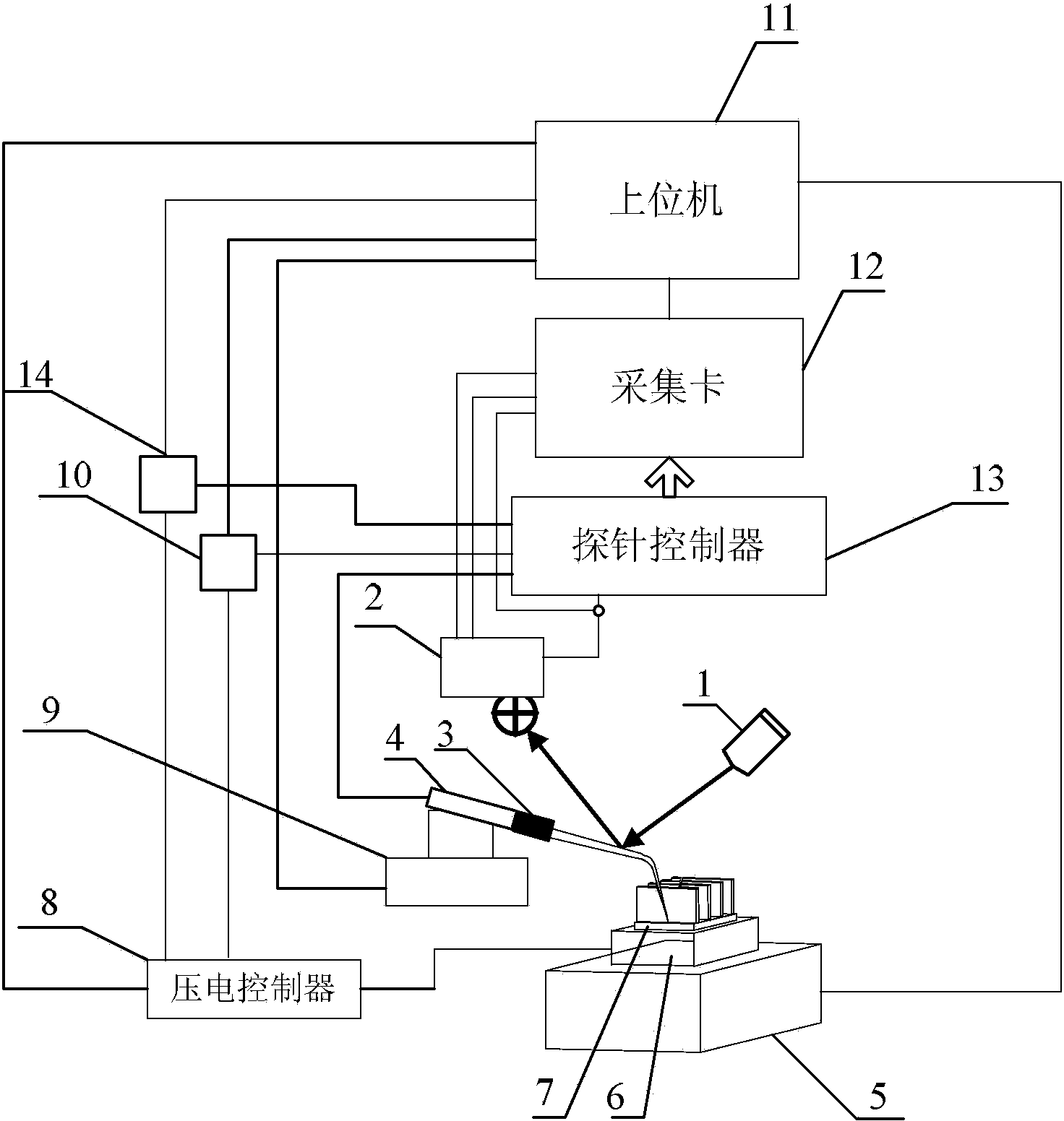
[0036] Specific implementation mode two: combination figure 1 This embodiment is described. This embodiment is a further limitation of the micro-nano structure side wall surface imaging device based on the atomic force microscope described in the first embodiment. In this embodiment, the atomic force microscope includes an optical microscope, a host computer 11, Laser mechanics subsystem, probe hand 4, XY micro-positioning stage 5, XYZ nano-positioning stage 6, sample stage 7 and XYZ micro-positioning stage 9, probe controller 13, acquisition card 12, piezoelectric controller 8, No. 1 Switcher 10 and No. 2 switcher 14;

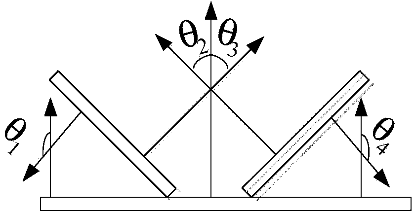
[0037] The laser mechanics subsystem is used to measure the interaction force signal or resonance signal between the probe and the sample surface, and the laser mechanics subsystem includes a laser 1 and a four-quadrant position detector 2;

[0038] The XY micro-positioning stage 5 is fixed on the base of the optical microscope, the base is a flat plate struc...

specific Embodiment approach 3

[0042] Specific Embodiment 3: This embodiment is a further limitation of the atomic force microscope-based micro-nano structure sidewall surface imaging device described in Embodiment 1. In this embodiment, the probe holder 3 also includes a transmission device 3- 2 and a knob, the transmission device 3-2 is arranged between the base 3-1 and the rotating arm 3-3, and the knob is used to adjust the transmission device 3-2, and then drive the rotating arm 3-3 to rotate.

[0043] In this embodiment, a transmission device 3-2 and a corresponding adjustment knob are added between the base 3-1 and the rotating arm 3-3. The angle is marked on the surface of the probe rack 3, and the transmission device 3-2 is adjusted by turning the adjusting knob, and then the angle of the rotating arm 3-3 is adjusted, so as to drive the probe at the front end of the rotating arm 3-3 to rotate, so that the probe Angle adjustment is more precise.


PUM


Abstract

A micro-nano structure sidewall surface imaging device based on an atomic force microscope and an imaging method thereof relate to a technology of using an AFM to carry out scanning imaging on a micro-nano structure sidewall surface, and are used for solving the problem that the conventional AFM is very difficult to carry out scanning imaging on the micro-nano structure sidewall surface. The micro-nano structure sidewall surface imaging device based on the atomic force microscope of the present invention is characterized in that a probe rack is added on the basis of the original atomic force microscope, so that a probe can rotate around an X-axis direction; in addition, a distance servo control program of a sample table in an XZ scanning plane is also added, so that the sample table can approach the tip of the probe along a Y direction, and reach a distance which is set by users. The micro-nano structure sidewall surface imaging device based on the atomic force microscope and the imaging method thereof of the present invention can select the appropriate probe rotation angle according to different samples, can carry out scanning imaging on the sidewall surface of a sample and represent the sidewall surface of the sample under the premise of not damaging the sample, thereby realizing the accurate representation of the sidewall surfaces of different samples. The micro-nano structure sidewall surface imaging device based on the atomic force microscope and the imaging method thereof of the present invention are applicable to the micro-nano structure surface representation, and also can be used in the micro-nano manufacture and test fields.

Description

technical field [0001] The invention relates to the technique of scanning and imaging the surface of the side wall of the micro-nano structure by using an atomic force microscope (AFM). Background technique [0002] Characterizing the sidewall surface of the micro-nano structure is an important means to detect the processing performance of the micro-nano structure. How to realize the characterization of the side wall surface of the micro-nano structure is the key to improving the detection technology of the micro-nano structure. The traditional atomic force microscope (AFM) adopts the Top-Down method to observe the surface morphology of the sample. This operation method can effectively observe the morphology of the surface parallel to the base surface and the surface inclined at a small angle to the base surface in the micro-nano structure. , but it is difficult to effectively observe the surface with a large acute angle to the base surface, the vertical side wall surface an...

Claims


Application Information

Patent Timeline
Patent Type & Authority Applications(China)
IPC IPC(8): G01Q60/24
Inventor 谢晖杨锋
Owner HARBIN INST OF TECH
Why Eureka
Try Eureka