Image collection device, liquid crystal terminal device and fingerprint and image collection method

A technology of image acquisition device and terminal equipment, which is applied in printing image acquisition, acquisition/organization of fingerprints/palmprints, instruments, etc. It can solve the problems of large camera size and achieve the effect of meeting the requirements of refinement, small thickness and reduced thickness

Active Publication Date: 2014-09-24
印象认知(东莞)科技有限公司
View PDF11 Cites 56 Cited by
  • Summary
  • Abstract
  • Description
  • Claims
  • Application Information

AI Technical Summary

Problems solved by technology

However, traditional cameras are large in size and cannot meet these requirements.

Method used


Image

  • Image collection device, liquid crystal terminal device and fingerprint and image collection method
  • Image collection device, liquid crystal terminal device and fingerprint and image collection method
  • Image collection device, liquid crystal terminal device and fingerprint and image collection method

Examples


Embodiment 1

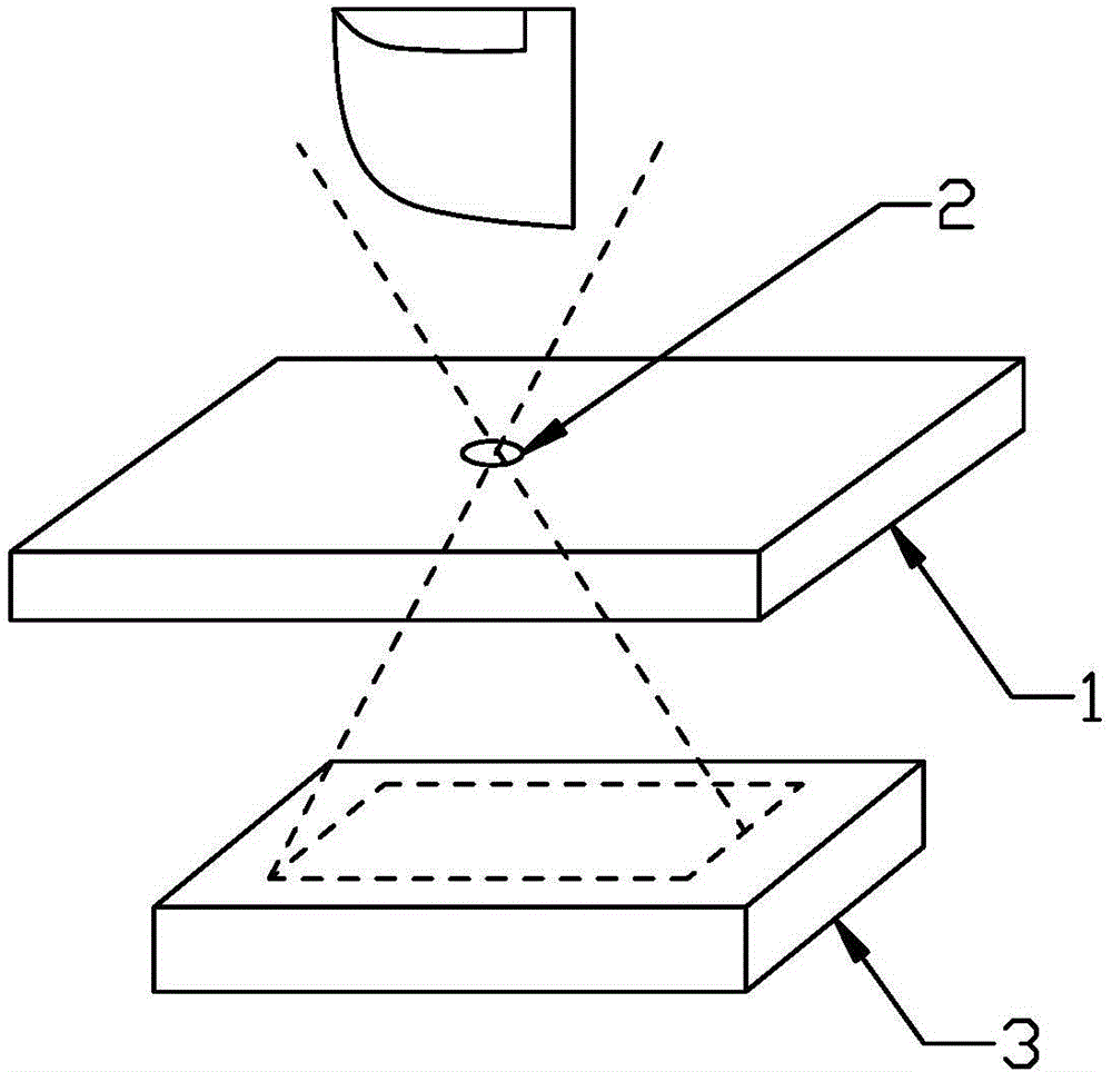
[0082] Such as figure 1 As shown, the collector includes a panel 1 with at least one imaging hole 2, and photoelectric conversion sensors 3 are arranged at intervals corresponding to the imaging holes. As shown in the figure, using the principle of pinhole imaging, the fingerprint can be imaged on the photoelectric conversion sensor through the imaging hole, thereby completing the collection of the fingerprint corresponding to the imaging hole. Wherein, the photoelectric conversion sensor can adopt photosensitive elements such as CMOS or CCD to collect fingerprints. figure 1 The basic principles on which the invention is based are shown.

Embodiment 2

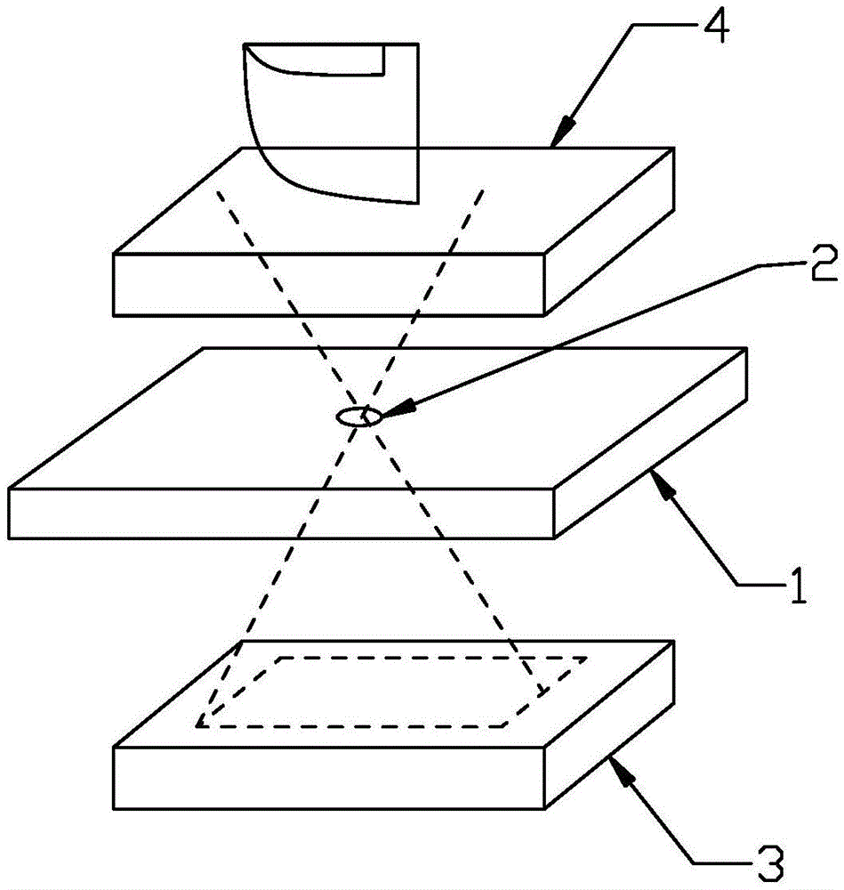
[0084] This embodiment is based on Embodiment 1: a transparent panel is added.

[0085] Such as figure 2 As shown, for some specific devices, a transparent panel 4 can be used to provide a touch surface for fingers, so as to facilitate fingerprint collection at a fixed resolution.

Embodiment 3

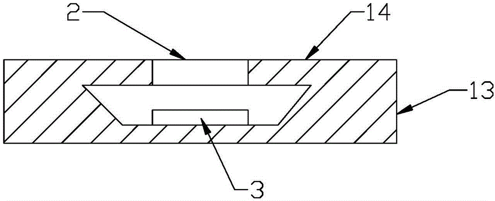
[0087] Such as image 3 As shown, the collector includes a box body 13 , the imaging hole is set on the front side panel 14 of the box body, and the photoelectric conversion sensor 3 is set at the bottom of the box body corresponding to the imaging hole 2 .

[0088] The above collector can be applied to various terminal devices. In application, the collector can be used as an independent module to collect fingerprints. In the above-mentioned embodiments, the aperture of the imaging hole can be 0.001-1mm; considering factors such as the best imaging effect and shorter imaging distance and processing, the aperture of the imaging hole should be selected at 0.01-0.2 Between mm, such as 0.1mm is better.


PUM


Abstract

The invention discloses an image collection device, a collector, a liquid crystal terminal device and a fingerprint and image collection method. On the basis of the pin-hole imaging principle, an ultrathin fingerprint collection instrument in any size can be formed, and the ultrathin fingerprint collection instrument can be further combined with a liquid crystal display screen to achieve the function of fingerprint collection; or, the ultrathin image collection device can be formed so as to collect images of universal targets. The liquid crystal terminal device comprises a liquid crystal display assembly. The liquid crystal display assembly is at least composed of a liquid crystal plate and a backlight module. The backlight module at least comprises a reflecting piece and a back plate. One or more imaging holes are formed in the reflecting piece and / or the back plate. Photovoltaic conversion sensors are arranged in the positions corresponding to the imaging holes. By conducting the structure improvement on the liquid crystal display screen according to the pin-hole imaging principle, the liquid crystal display screen can collect fingerprints and support the terminal device to complete screen unlocking, account verification and other operation needing personal identity authentication through fingerprint identification.

Description

technical field [0001] The invention relates to an image acquisition device, an acquisition device, a liquid crystal terminal equipment and a fingerprint and image acquisition method for a liquid crystal panel. Background technique [0002] At present, there are mainly two methods for the collection of fingerprints and images. One is based on semiconductor chips to directly collect fingerprints; the other is an optical collection method based on the principle of total reflection. Both approaches have their pros and cons. The size of traditional optical fingerprint collection equipment is large, and it is difficult to meet the requirements of mobile devices for thickness and size; while the semiconductor chip fingerprint collection method has shortcomings such as insufficient antistatic and anti-corrosion capabilities. [0003] Cameras are a common device with important applications in various industries. The camera generally consists of an optical lens group, a shutter de...

Claims


Application Information

Patent Timeline
Patent Type & Authority Applications(China)
IPC IPC(8): G06K9/20G06K9/00
CPCG06V40/1318
Inventor 张明方
Owner 印象认知(东莞)科技有限公司
Why Eureka
Try Eureka