Transistors and methods of forming them

A transistor and semiconductor technology, applied in semiconductor devices, semiconductor/solid-state device manufacturing, electrical components, etc., can solve problems such as unfavorable system integration, high power consumption of transistors, and achieve improved carrier mobility, reduced power consumption, and thresholds The effect of voltage stabilization

Active Publication Date: 2017-06-09
SEMICON MFG INT (SHANGHAI) CORP
View PDF1 Cites 0 Cited by
  • Summary
  • Abstract
  • Description
  • Claims
  • Application Information

AI Technical Summary

Problems solved by technology

[0004] However, as the feature size of transistors continues to shrink, the threshold voltage VT of transistors cannot be reduced accordingly, resulting in excessive power consumption of transistors, which is not conducive to system integration

Method used


Image

  • Transistors and methods of forming them
  • Transistors and methods of forming them
  • Transistors and methods of forming them

Examples


Embodiment Construction

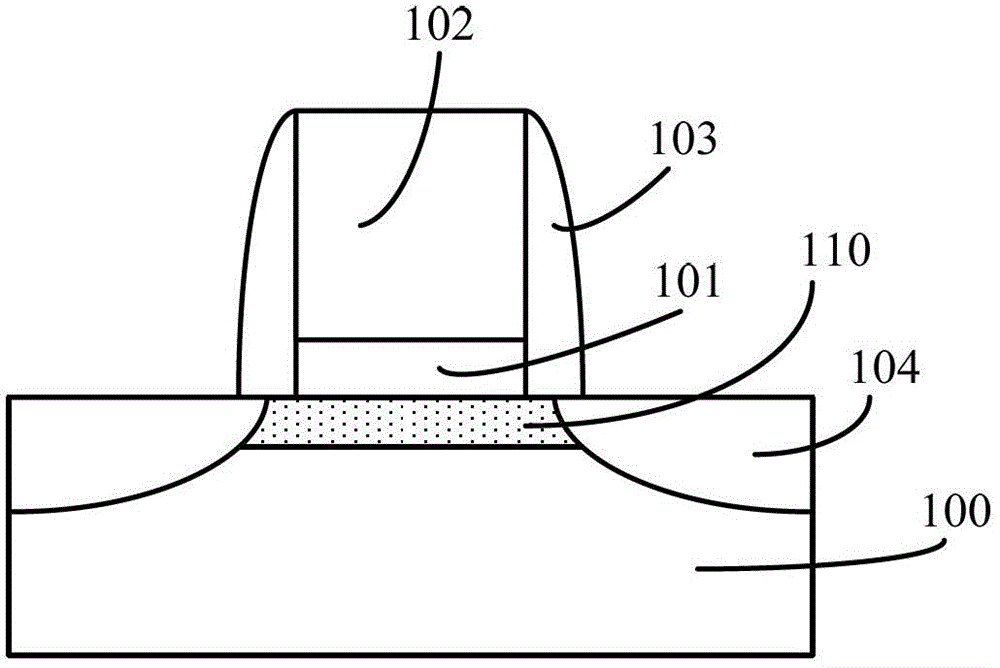
[0034] As mentioned in the background, although the feature size of the transistor is continuously reduced, the threshold voltage V of the transistor T However, it cannot be reduced accordingly, resulting in excessive power consumption of the transistor.

[0035]The inventors of the present invention have found through research that, as the feature size of the transistor shrinks, the size of the channel region of the transistor also decreases accordingly, making the dopant ions in the channel region more sensitive to the influence of the threshold voltage. Specifically, the dopant ions in the channel region can generate random dopant fluctuations (RDF, Random Dopant Fluctuations) effect, and the random dopant fluctuation effect will generate a threshold voltage deviation σV T , and the threshold voltage deviation σV T The value of increases with the decrease of channel region size. The threshold voltage deviation σV T The turn-on voltage of different transistors will be dif...


PUM


Abstract

The invention provides a transistor and a formation method thereof. The formation method of the transistor comprises: providing a semiconductor substrate, wherein the surface of the semiconductor substrate is provided with a plurality of separating layers, openings are formed between neighboring separating layers, the bottoms of the openings are provided with threshold voltage adjusting layers, and the threshold voltage adjusting layers are internally provided with doped ions; forming barrier layers on the surfaces of the threshold voltage adjusting layers and channel layers on the surfaces of the barrier layers, wherein the channel layers are at intrinsic states, and the barrier layers are used for preventing penetration by the doped ions in the threshold voltage adjusting layers; forming grid structures on the surfaces of the channel layers, wherein the surfaces of the grid structures are flush with the surfaces of the separating layers; removing the separating layers until the semiconductor substrate is exposed; and after the separating layers are removed, forming a doping layer on the surface of the semiconductor substrate at the two sides of the threshold voltage adjusting layers, the separating layers, the channels layers and the grid structures, wherein the surface of the doping layer is not lower than the surfaces of the channel layers. The formed transistor is lower in power consumption and stable in performance.

Description

technical field [0001] The invention relates to the technical field of semiconductor manufacturing, in particular to a transistor and a forming method thereof. Background technique [0002] With the rapid development of integrated circuit manufacturing technology, the size of semiconductor devices in integrated circuits, especially MOS (Metal Oxide Semiconductor, metal-oxide-semiconductor) devices, has been continuously reduced to meet the miniaturization and development of integrated circuits. Integration requirements. In the process of continuous shrinking of the size of MOS transistor devices, the process of using silicon oxide or silicon oxynitride as the gate dielectric layer in the existing process is challenged. Transistors formed with silicon oxide or silicon oxynitride as the gate dielectric layer have some problems, including increased leakage current and diffusion of impurities, which affect the threshold voltage of the transistor and further affect the performan...

Claims


Application Information

Patent Timeline
Patent Type & Authority Patents(China)
IPC IPC(8): H01L21/336H01L29/78H01L29/10
CPCH01L29/0607H01L29/1033H01L29/6653H01L29/78
Inventor 赵猛
Owner SEMICON MFG INT (SHANGHAI) CORP
Why Eureka
Try Eureka