Field effect transistor and process for production thereof

a field effect transistor and transistor technology, applied in the direction of semiconductor/solid-state device details, electrical equipment, semiconductor devices, etc., can solve the problems of difficult formation of thin films on substrates, less reliable, and gold does not have sufficient adhesiveness to an oxide semiconductor

Inactive Publication Date: 2012-04-24
CANON KK
View PDF26 Cites 107 Cited by
  • Summary
  • Abstract
  • Description
  • Claims
  • Application Information

AI Technical Summary

Benefits of technology

[0025]The field effect transistor of the present invention employs an oxide semiconductor as the channel layer, and an oxynitride as the source electrode and / or the drain electrode, which stabilizes the electric connection between the channel region and the source electrode and / or drain electrode and improves the uniformity and reliability of the elements.
[0026]Further, the electrode constituted of an oxynitride absorbs near-ultraviolet light to prevent penetration of the near-ultraviolet light through the source electrode portion or the drain electrode portion. Thus the constitution of the present invention prevents variation of the TFT characteristics even when stray light is generated within the TFT substrate (substrate on which an array of TFTs is formed), and provides a TFT substrate which has stable characteristics against irradiation of near-ultraviolet light.

Problems solved by technology

However, the amorphous silicon TFT or the polysilicon TFT is necessarily processed at a high temperature in the device production, which makes difficult the formation of the thin film on a substrate like a plastic substrate or a film.
A noble metal such as gold does not have sufficient adhesiveness to an oxide semiconductor, and is less reliable in that the metal electrode produced by a productive process like vacuum deposition or sputtering is easy to be peeled off.
However, the surface property of such an oxide electrode can be affected in the film forming process or the post-treatment including a heat treatment and a solution treatment to cause variation in electric connection with the semiconductor.
Display device using the transistor tends to cause deterioration of the image quality on irradiation of a display light or an external light onto the TFT.
This will limit the layout of the TFT and increase the production steps.
Further, even with the light-shielding layer, depending on the constitution, a trace amount of stray light can irradiate the TFT, unexpectedly.

Method used


Image

  • Field effect transistor and process for production thereof
  • Field effect transistor and process for production thereof
  • Field effect transistor and process for production thereof

Examples


example 1

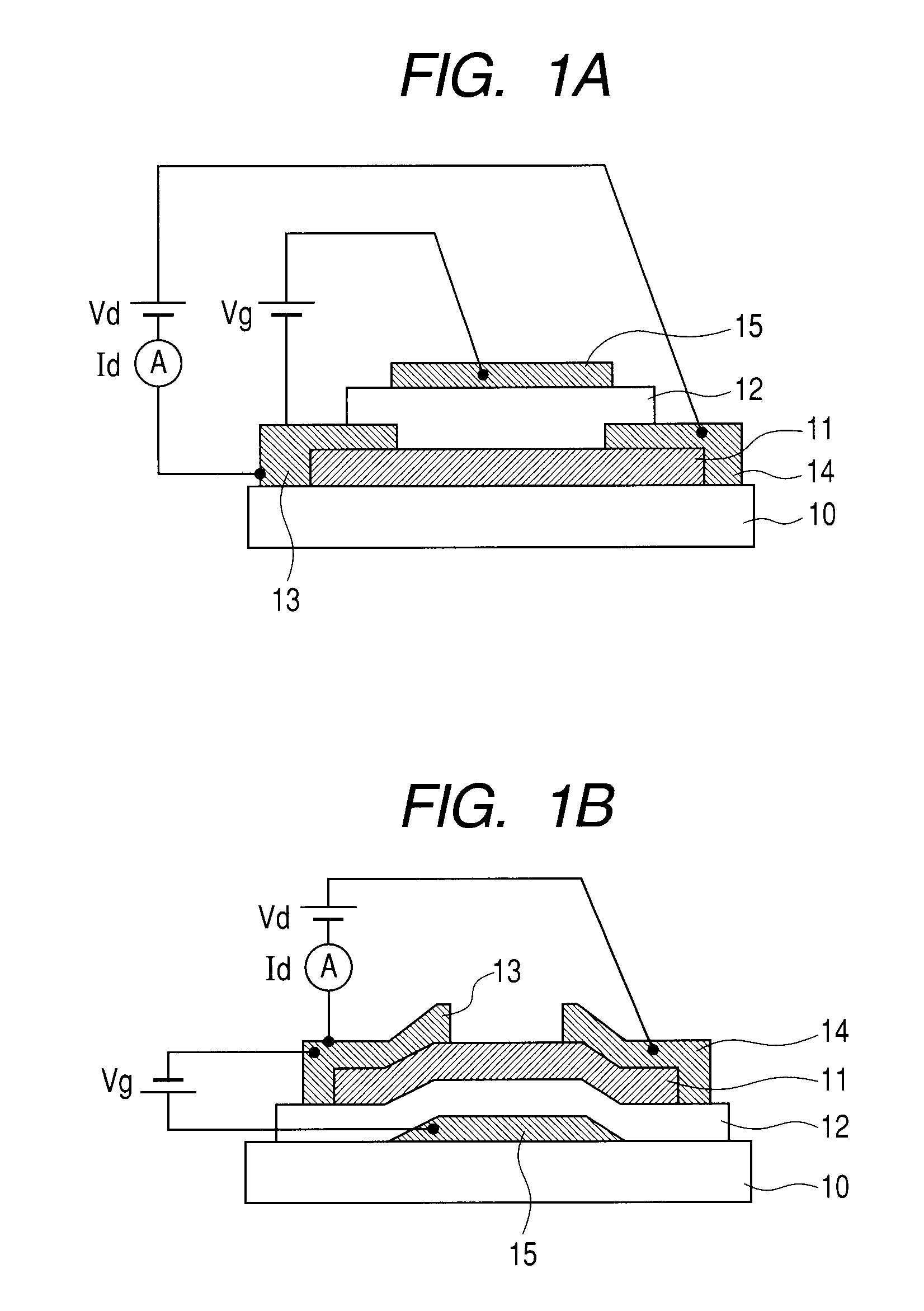
[0068]FIG. 1A illustrates a top-gate type TFT of this Example. Channel layer 11 is a film of an amorphous oxide semiconductor of In—Ga—Zn—O type. Source electrode 13 and drain electrode 14 are films of an oxynitride of an In—Ga—Zn—O—N type. A process for producing such a TFT is described below.

[0069]Firstly, an amorphous oxide semiconductor layer is formed as channel layer 11 on glass substrate 10 (made by Corning Co.: 1737). In this Example, the amorphous oxide film of an In—Ga—Zn—O type is formed by radio frequency sputtering method in an atmosphere of an argon-oxygen gas mixture. The sputtering is conducted by use of, as the target (material source), a polycrystalline sintered compact of InGaZnO4 in a size of 2 inches with the RF power input of 100 W, in an atmosphere of a gas mixture of Ar:O2 (flow rate ratio of 100:1) at a total gas pressure of 0.45 Pa at the substrate temperature of 25° C. The film deposition rate is 12 nm / min. After forming the film, the annealing is carried ...

example 2

[0081]FIG. 1B illustrates a bottom-gate type TFT of this Example. Channel layer 11 is a film of an amorphous oxide of Zn—In—O type. Source electrode 13 and drain electrode 14 are films of an oxynitride of a Zn—In—O—N type. A process for producing such a TFT is described below.

[0082]Firstly, a Mo film is formed in a thickness of 100 nm as the gate electrode on a glass substrate (made by Corning Co.: 1737) by sputtering.

[0083]Then a SiOx film is formed as gate electrode-insulating layer 12 in a thickness of 150 nm by sputtering.

[0084]Thereafter an amorphous oxide semiconductor film of a Zn—In—O type is formed as the channel layer by simultaneous sputtering by use of a ZnO target and an In2O3 target. In the sputtering, the mixing ratio of argon and oxygen is Ar:O2=80:1, film formation rate is 12 nm / min, the substrate temperature is 25° C., and the film thickness is about 30 nm. The formed Zn—In—O film is amorphous. The metal compositional ratio of Zn:In is 64:36. The thin film has no d...

example 3

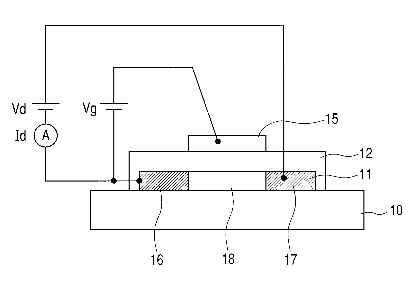
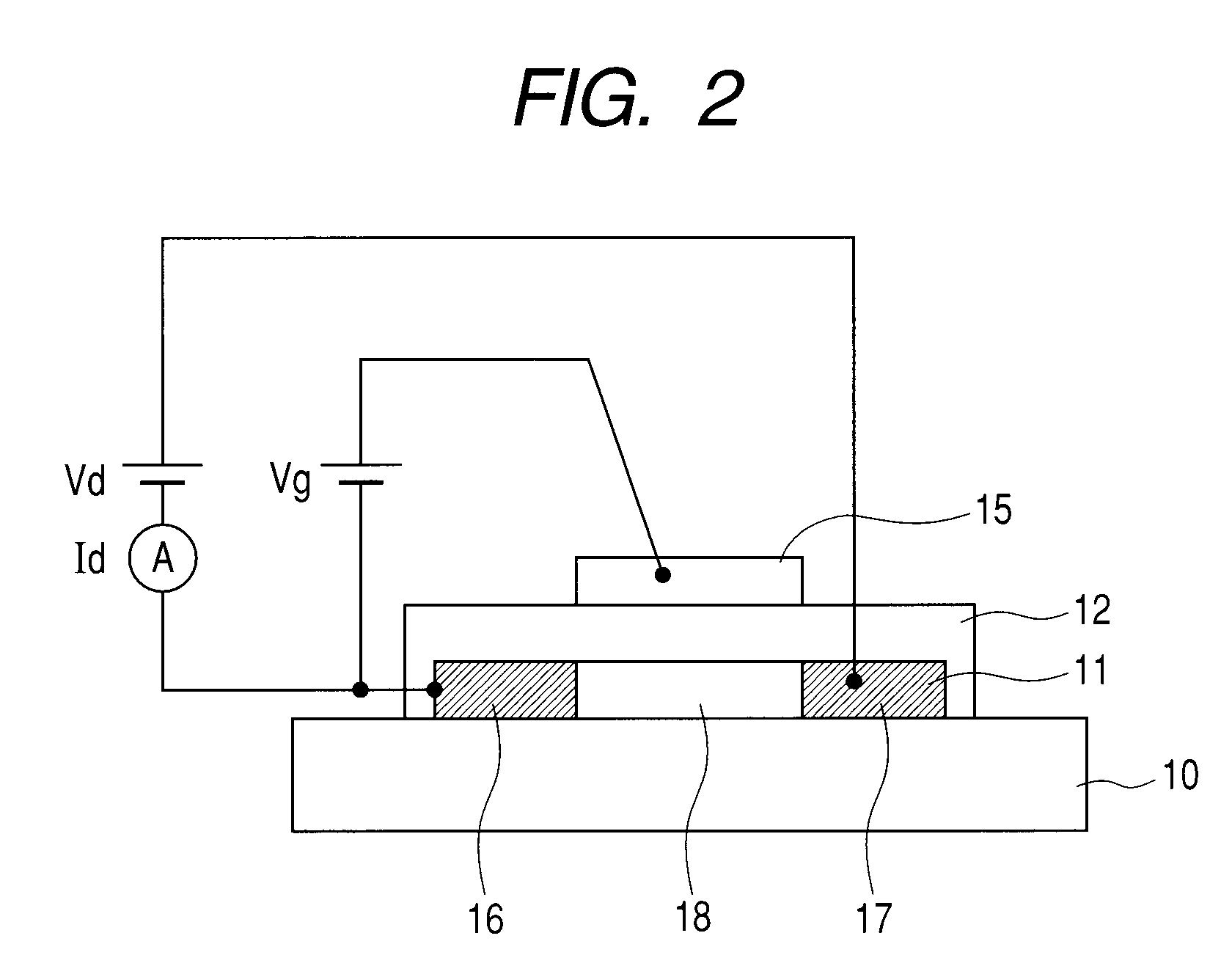
[0091]FIG. 2 illustrates a coplanar type of the field effect transistor of this Example. FIG. 2 is a sectional view, in which the reference numerals denote the followings: 10, a substrate; 11, a channel layer (oxide thin film); 12, a gate insulating layer; and 15, a gate electrode. Channel layer 11 has three regions: source region 16 containing implanted nitrogen (corresponding to the source electrode in Example 1), drain region 17 containing implanted nitrogen (corresponding to the drain electrode in Example 1), and channel region 18 (corresponding to the channel layer in Example 1). Channel layer 11 is formed from In—Ga—Zn—O type amorphous oxide, and source region 16 and drain region 17 as the electrodes are formed therein by nitrogen ion implantation. FIGS. 7A, 7B, and 7C illustrate a process of formation of the source region and the drain region. The steps of formation of such a transistor are described below.

[0092]Firstly, an amorphous oxide layer is formed as channel layer 11 ...


PUM


Abstract

A field effect transistor has a gate electrode, gate-insulating layer, a channel and a source and drain electrodes connected electrically to the channel, the channel comprising an oxide semiconductor, the source electrode or the drain electrode comprising an oxynitride.

Description

BACKGROUND OF THE INVENTION[0001]1. Field of the Invention[0002]The present invention relates to a field effect transistor employing a semiconductor film composed of an oxide as the channel. The present invention relates also to a process for producing the transistor.[0003]2. Description of the Related Art[0004]The field effect transistor (FFT) is a three-terminal element comprising a gate electrode, a source electrode, and a drain electrode. This FET is an electron-active element for controlling and switching, by application of a voltage to a gate electrode, the current flowing through the channel layer between the source electrode and the drain electrode. In particular, the FET employing a semiconductor thin film as a channel layer is called a thin film transistor (TFT).[0005]The TFT, based on the thin film technique, can readily be formed in a large area on a substrate advantageously. Therefore, the TFTs are widely used as a driving element of a flat panel display like a liquid c...

Claims


Application Information

Patent Timeline
Patent Type & Authority Patents(United States)
IPC IPC(8): H01L29/72
CPCH01L29/78618H01L29/7869H01L29/45
Inventor IWASAKI, TATSUYAITAGAKI, NAHO
Owner CANON KK
Why Eureka
Try Eureka