Sensor device

a technology of a sensor and a spherical device, which is applied in the direction of turn-sensitive devices, semiconductor/solid-state device details, instruments, etc., can solve the problem of restricting the variation in and achieve the effect of restricting the parasitic capacity of the electric connection portion

Inactive Publication Date: 2006-05-11
DENSO CORP
View PDF3 Cites 95 Cited by
  • Summary
  • Abstract
  • Description
  • Claims
  • Application Information

AI Technical Summary

Benefits of technology

[0011] In view of the above-described problems, it is an object of the present invention to effectively restrict parasitic capacity of an electric connecting portion of two chips from being changed by an impact, etc. in a sensor device constructed by laminating a sensor chip having a movable portion on one surface and a circuit chip and electrically connecting both the chips.

Problems solved by technology

Further, both the chips are electrically connected through the bump, a deformation of an electrical connection portion between both the chips can be restricted, thereby effectively restrict a variation in parasitic capacity of the electric connection portion due to an impact.

Method used


Image

  • Sensor device
  • Sensor device
  • Sensor device

Examples


first embodiment

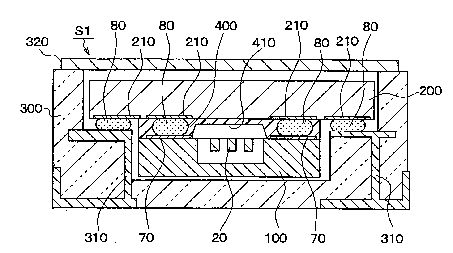
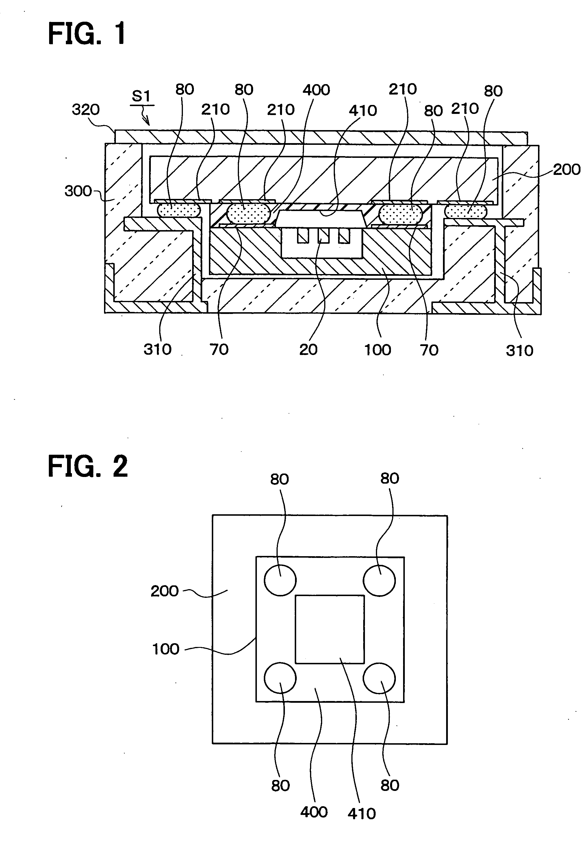
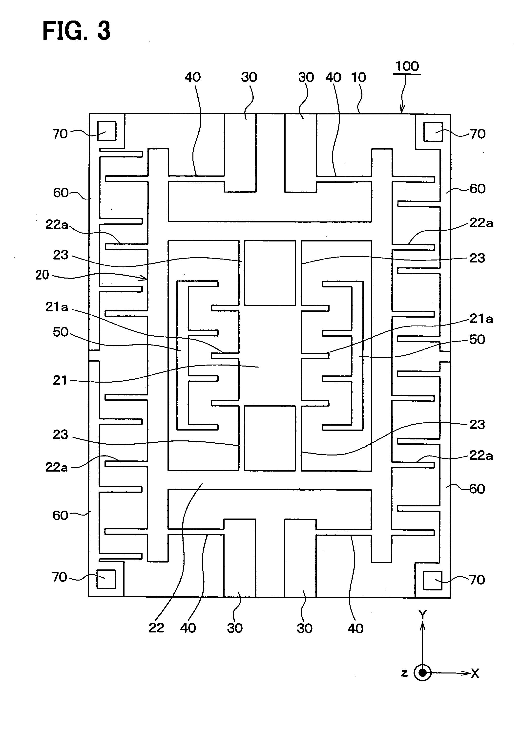
[0035]FIG. 1 is a view showing an entire structure of an angular velocity sensor device S1 as a sensor device in accordance with the first embodiment of the present invention. FIG. 2 is a schematic plan view showing a surface structure of a circuit chip 200 having bumps 80 in the angular velocity sensor device S1 shown in FIG. 1 in a transmitting state of a sensor chip 100. FIG. 3 is a view showing a schematic planar structure of an angular velocity detecting element 100 in the angular velocity sensor device S1 shown in FIG. 1 when being viewed from the upper surface of a substrate 10 constituting this element 100.

[0036] As shown in FIG. 1, the angular velocity sensor device S1 of this embodiment is generally formed by arranging the angular velocity detecting element 100 as the sensor chip, the circuit chip 200, and a package 300 for accommodating the angular velocity detecting element 100 and the circuit chip 200.

[0037] First, the angular velocity detecting element 100 will be ma...

second embodiment

[0120]FIG. 11 is a view showing an angular velocity sensor device S2 as a sensor device in accordance with a second embodiment of the present invention.

[0121] In this embodiment, as shown in FIG. 11, similarly to the above first embodiment, in the angular velocity sensor device S2, an angular velocity detecting element (sensor chip) 100 having a vibrator 20 on one surface and a circuit chip 200 are laminated and both these chips 100, 200 are electrically connected. Furthermore, the angular velocity detecting element 100 is laminated with the circuit chip 200 through bumps 80 such that its vibrator 20 is opposed to the circuit chip 200. In addition, both the chips 100, 200 are electrically connected by the bump 80, while the vibrator 20 and the circuit chip 200 are separated by a space through the bumps 80.

[0122] Here, as shown in FIG. 11, in the angular velocity sensor device S2 of this embodiment, the above-described adhesive member is not arranged between the angular velocity de...

third embodiment

[0126]FIG. 12 is a view showing a part of an angular velocity sensor device S3 as a sensor device in accordance with a third embodiment of the present invention.

[0127] In the third embodiment, as shown in FIG. 12, similarly to the above first embodiment, in the angular velocity sensor device S3, an angular velocity detecting element (sensor chip) 100 having a vibrator 20 on one surface and a circuit chip 200 are laminated and both these chips 100, 200 are electrically connected. In addition, the angular velocity detecting element 100 is laminated with the circuit chip 200 through bumps 80 in a state in which its vibrator 20 is opposed to the circuit chip 200, and both the chips 100, 200 are electrically connected by the bumps 80, and the vibrator 20 and the circuit chip 200 are separated by the bumps 80.

[0128] Further, an adhesive member 400 having an electric insulating property for adhering both these chips 100, 200 is arranged between the angular velocity detecting element 100 ...


PUM


Abstract

A sensor device includes a sensor chip having a movable portion on one surface, a circuit chip laminated with the sensor chip to be opposite to the movable portion of the sensor chip, and a bump located between the sensor chip and the circuit chip. In the sensor device, the sensor chip and the circuit chip are electrically connected through the bump, and the movable portion of the sensor chip is separated from the circuit chip by a space using the bump. Accordingly, it can effectively restrict parasitic capacity of an electric connecting portion between both the chips from being changed by an impact. For example, the sensor device can be used as an angular velocity sensor device having a vibrator as the movable portion.

Description

CROSS REFERENCE TO RELATED APPLICATION [0001] This application is based on Japanese Patent Applications No. 2004-352741 filed on Dec. 6, 2004, and No 2005-277696 filed on Sep. 26, 2005, the contents of which are incorporated herein by reference in its entirety.FIELD OF THE INVENTION [0002] The present invention relates to a sensor device in which a sensor chip having a movable portion as a sensing portion on one surface and a circuit chip are laminated, and both the chips are electrically connected. In particular, the present invention relates to a sensor device for detecting a dynamic amount such as angular velocity, acceleration, etc. by a movable portion. BACKGROUND OF THE INVENTION [0003] In a sensor device having a sensor chip, in which a movable portion displaced by a dynamic amount such as acceleration, angular velocity or pressure, etc. is formed on one surface side of a semiconductor substrate. [0004] For example, an angular velocity sensor having a vibrator constructed wit...

Claims


Application Information

Patent Timeline
Patent Type & Authority Applications(United States)
IPC IPC(8): H01L29/82G01C19/56G01C19/5762G01C19/5769G01P15/08H01L25/065H01L25/07H01L25/18H01L29/84
CPCG01C19/5719G01P1/023G01P15/125H01L2224/48091H01L2224/73265H01L2924/1305H01L2924/13091H01L2924/00014H01L2924/00B81C1/0023B81C1/00238
Inventor HATTORI, KOJIYONEYAMA, TAKAOABE, RYUICHIROSAKAI, MINEKAZUYAMAUCHI, SHIGENORI
Owner DENSO CORP
Why Eureka
Try Eureka