Device package structure with heat radiating structure and manufacturing method thereof

A technology of device packaging and heat dissipation structure, applied in semiconductor/solid-state device manufacturing, semiconductor devices, electric solid-state devices, etc., can solve the problems of high cost of flip-chip plastic packaging structure, poor signal shielding effect, poor grounding performance, etc. Effective heat dissipation and normal operation, good grounding performance and low cost

Inactive Publication Date: 2014-09-24
INST OF MICROELECTRONICS CHINESE ACAD OF SCI +1
View PDF6 Cites 5 Cited by
  • Summary
  • Abstract
  • Description
  • Claims
  • Application Information

AI Technical Summary

Problems solved by technology

[0007] Embodiments of the present invention provide a device packaging structure with a heat dissipation structure and a manufacturing method, which are used to solve the problems of high cost, poor heat dissipation capability, poor grounding performance, and poor signal shielding effect of flip-chip plastic packaging structures in the prior art problem, with low cost, good heat dissipation performance, good grounding performance, and good signal shielding effect

Method used


Image

  • Device package structure with heat radiating structure and manufacturing method thereof
  • Device package structure with heat radiating structure and manufacturing method thereof
  • Device package structure with heat radiating structure and manufacturing method thereof

Examples


Embodiment 1

[0028] In order to enable those skilled in the art to understand the present invention in more detail, the present invention will be described in detail below in conjunction with the accompanying drawings.

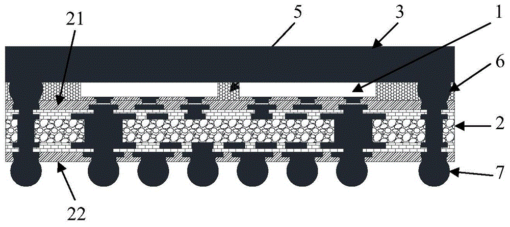
[0029] Such as figure 1 said, figure 1 It is a flip-chip plastic packaging structure with a heat dissipation structure in an embodiment of the present invention, wherein the structure includes:

[0030] Chip 1;

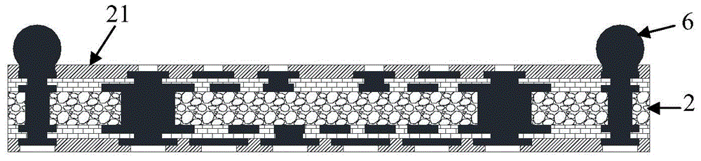
[0031] A substrate 2, the first surface 21 of the substrate 2 is provided with the chip;

[0032] Height-limiting bumps 6, the height-limiting bumps 6 are arranged on the first surface 21 of the substrate 2;

[0033] A heat dissipation plate 3, the heat dissipation plate 3 is arranged on the chip 1 and the height-limiting bump 6, and the heat dissipation plate 3 is connected to the first surface 21 of the substrate 2, the height-limiting bump 6, The chip 1 forms a first space 4; the height-limiting bump 6 is connected to the heat dissipation plate 3, so that t...

Embodiment 2

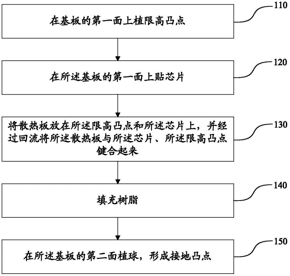
[0045] Such as Figure 2-8 As shown, the embodiment of the present invention also provides a method for manufacturing a device package with a heat dissipation structure, the method comprising:

[0046] Step 110: planting height-limiting bumps 6 on the first surface 21 of the substrate 2;

[0047] Step 120: paste the chip 1 on the first surface 21 of the substrate 2;

[0048] Step 130: Put the cooling plate 3 on the height-limiting bump 6 and the chip 1, and bond the cooling plate 3, the chip 1, and the height-limiting bump 6 through reflow;

[0049] Step 140: filling the molding resin 5;

[0050] Step 150 : Plant balls on the second surface 22 of the substrate 2 to form ground bumps 7 .

[0051] Further, the step 140 of filling the molding resin 5 also includes:

[0052] Plastic material is poured into the encapsulation by capillary action.

[0053] Eliminate air bubbles during the potting process by vacuum exhaust.

[0054] Further, in step 130, place the heat dissipati...


PUM


Abstract

The invention discloses a device package structure with a heat radiating structure and a manufacturing method thereof. Through setting a chip and height limitation convex points on the first surface of a substrate, a first space is formed by a heat radiating plate, the first surface of the substrate, the height limitation convex points and the chip, plastic resin is filled in the first space, the height limitation convex points are connected with the heat radiating plate, thus the ground electrode of the substrate is connected with the heat radiating plate through the height limitation convex points, electric shielding is formed, and technical effects of low cost, good heat radiating performance, good grounding performance, and good signal shielding effect are achieved.

Description

technical field [0001] The invention relates to the technical field of semiconductors, in particular to a device packaging structure with a heat dissipation structure and a manufacturing method. Background technique [0002] In the field of semiconductor technology, the commonly used flip-chip plastic packaging structure and method are usually to flip-chip solder the chip on the substrate, then fill it with glue, and then perform plastic packaging through a mold, and then encapsulate the entire chip with resin. Bumping is done on the backside of the substrate to complete the entire packaging process. [0003] But, those skilled in the art find that there is following deficiency in the prior art through research: [0004] 1. Although this plastic packaging structure and method is simple and easy to mass-produce, it needs to make high-precision molds, and for different packaging heights, different molds need to be manufactured. Due to the high cost of mold manufacturing, the ...

Claims


Application Information

Patent Timeline
Patent Type & Authority Applications(China)
IPC IPC(8): H01L23/31H01L23/367H01L21/56
CPCH01L2224/16227H01L2224/32245H01L2224/73253H01L2224/92225H01L2924/1533H01L2924/15331H01L2924/3025
Inventor 于中尧郭学平
Owner INST OF MICROELECTRONICS CHINESE ACAD OF SCI
Why Eureka
Try Eureka