Light-emitting diode, package substrate structure and packaging method

A technology for light-emitting diodes and packaging substrates, which is applied to electrical components, electrical solid-state devices, circuits, etc., can solve the problems of increasing the cost and difficulty of manufacturing the light-emitting diode 1, and being unable to perform full-angle 360° lighting, thereby reducing the complexity of the process. , to avoid the effect of the wire bonding process

Inactive Publication Date: 2014-09-24
ENRAYTEK OPTOELECTRONICS
View PDF4 Cites 0 Cited by
  • Summary
  • Abstract
  • Description
  • Claims
  • Application Information

AI Technical Summary

Problems solved by technology

However, this will increase the manufacturing process cost and difficulty of LED 1
During the encapsulation process of the photodiode 1, the photodiode 1 is generally pasted on the bracket through silica gel, and the light emitted by the light-emitting diode 1 is emitted through the light-transmitting protective layer 3 (usually a lens). Since the bracket is opaque, light is emitted from one side after packaging. The light-emitting angle of the light-emitting diode 1 is limited to about 110°, and it is impossible to perform full-angle 360° illumination

Method used


Image

  • Light-emitting diode, package substrate structure and packaging method
  • Light-emitting diode, package substrate structure and packaging method
  • Light-emitting diode, package substrate structure and packaging method

Examples


Embodiment Construction

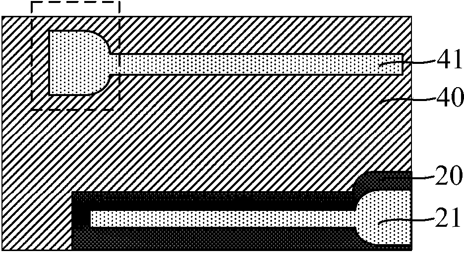
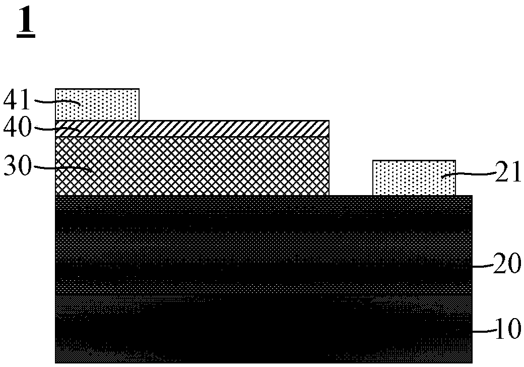
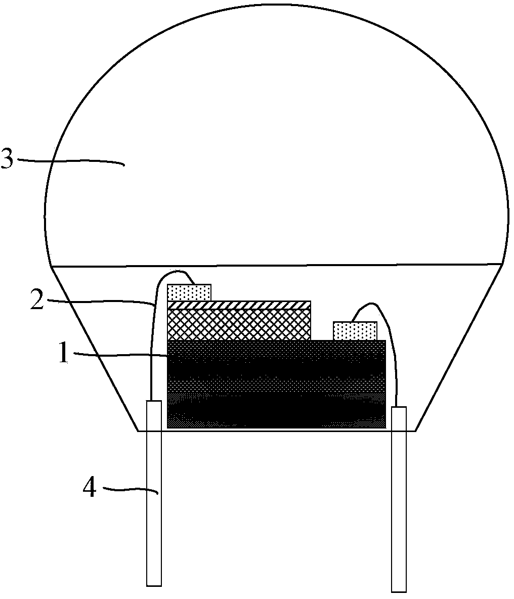
[0034] The light-emitting diode, packaging substrate structure and packaging method of the present invention will be described in more detail below in conjunction with schematic diagrams, wherein a preferred embodiment of the present invention is shown, and it should be understood that those skilled in the art can modify the present invention described here and still achieve Advantageous effects of the present invention. Therefore, the following description should be understood as the broad knowledge of those skilled in the art, but not as a limitation of the present invention.

[0035] In the interest of clarity, not all features of an actual implementation are described. In the following description, well-known functions and constructions are not described in detail since they would obscure the invention with unnecessary detail. It should be appreciated that in the development of any actual embodiment, numerous implementation details must be worked out to achieve the develo...


PUM


Abstract

The invention provides a light-emitting diode, a package substrate structure and a packaging method. The connection end of a P-type electrode of the light-emitting diode and the connection end of an N-type electrode of the light-emitting diode are installed at the same end. Meanwhile, a slot is formed in the package substrate structure, and connection metal is installed in the slot. When packaging is carried out, the end, provided with the connection ends, of the light-emitting diode is inserted in the slot in the package substrate structure, a routing process is omitted, and meanwhile 360-degree light emitting of the light-emitting diode can be achieved. No DBR structure is needed, and process complexity is reduced.

Description

technical field [0001] The invention relates to the field of light-emitting diode manufacturing, in particular to a light-emitting diode, a packaging substrate structure and a packaging method. Background technique [0002] LED (Light-Emitting Diode, light-emitting diode) devices based on GaN (gallium nitride) materials have been widely used in production and daily life, and are mainly used to emit blue light and green light. LED devices based on GaN materials usually use N-type doped GaN, InGaN (indium gallium nitride) quantum wells and P-type doped GaN. After biasing at both ends, P-type doped GaN provides hole carriers. , N-type doped GaN provides electron carriers, electrons and holes flow in reverse, and recombination occurs in the InGaN quantum well, thereby emitting light of a certain wavelength. Among the many factors that affect the luminous efficiency of the device, the metal electrodes at both ends used for voltage application should form a good ohmic contact wit...

Claims


Application Information

Patent Timeline
Patent Type & Authority Applications(China)
IPC IPC(8): H01L33/38H01L33/48H01L33/62
CPCH01L33/38H01L33/62H01L2933/0016H01L2933/0066H01L33/42H01L33/44H01L33/483H01L33/486H01L2224/48091H01L2224/49107H01L2933/0033H01L2933/005H01L2924/00014
Inventor 张宇
Owner ENRAYTEK OPTOELECTRONICS
Why Eureka
Try Eureka