

Wafer-level preparation method of photosensitive module and structure of lens module
A photosensitive module and wafer-level technology, applied in radiation control devices, color TV components, TV system components, etc., can solve problems such as long process time, high cleanliness requirements, and low packaging costs
- Summary
- Abstract
- Description
- Claims
- Application Information
AI Technical Summary
Problems solved by technology
Method used
Image

Examples
Embodiment approach
[0043] like figure 1 As shown, according to an embodiment of the present invention, a wafer-level manufacturing method of a photosensitive module is provided, comprising the following steps:
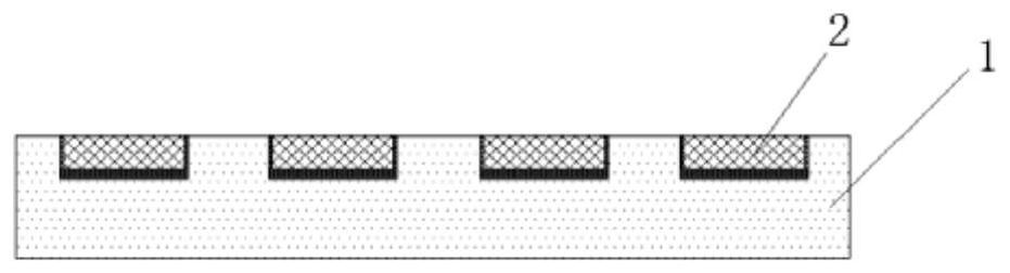
[0044] Step 1: As shown in FIG. 2(A), provide a first wafer 1 formed with a plurality of photosensitive elements 2, and a photosensitive area is provided on the photosensitive element 2, which can be formed on the first wafer 1 in a variety of known ways. The photosensitive element 2 is formed.
[0045] As an example, the photosensitive element 2 is a CCD (Charge Coupled) element or a CMOS (Complementary Metal Oxide Semiconductor) device.
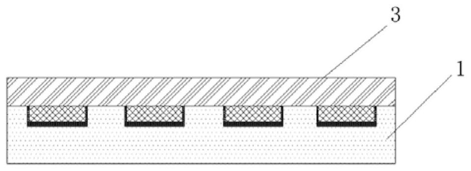
[0046] Step 2: as shown in FIG. 2(B), temporarily bond the second carrier substrate 3 on the front side of the first wafer 1; and thin the back side of the first wafer 1, as shown in FIG. 2(C). Show.
[0047] The thinning process can use any suitable mechanical grinding process, chemical mechanical grinding process or etching process. The thicknes...
PUM
 Abstract
Description
Claims
Application Information