Copper pillar spacer with stress buffer and anisotropic conduction and method of making the same

An anisotropic, stress-buffering technology, applied in semiconductor/solid-state device manufacturing, circuits, electrical components, etc., can solve problems such as downward offset, offset reduction, and increased cost

Active Publication Date: 2021-05-14
TIANJIN UNIV
View PDF9 Cites 0 Cited by
  • Summary
  • Abstract
  • Description
  • Claims
  • Application Information

AI Technical Summary

Problems solved by technology

When the gate of the chip is not located at the corner of the chip, in order to increase the allowable current value as much as possible, it is necessary to design and process metal pillars with complex shapes and structures. On the one hand, it increases the difficulty of operation, and on the other hand, it also increases the cost.
[0004] In a module where multiple chips are connected in parallel and independently controlled between chips, multiple metal pillars need to be used to achieve a double-sided structure. A downward contraction force will be generated when the point is solidified, but each solder joint is not solidified at the same time, which will cause the area where the solder joint solidifies first to be subjected to the contraction force and shift downward, and will be displaced when other solder joints solidify The hindrance of the solidified solder joint reduces the downward offset, which eventually leads to a certain angle of deviation between the upper and lower direct copper clad substrates (DBC)

Method used


Image

  • Copper pillar spacer with stress buffer and anisotropic conduction and method of making the same
  • Copper pillar spacer with stress buffer and anisotropic conduction and method of making the same
  • Copper pillar spacer with stress buffer and anisotropic conduction and method of making the same

Examples


Embodiment Construction

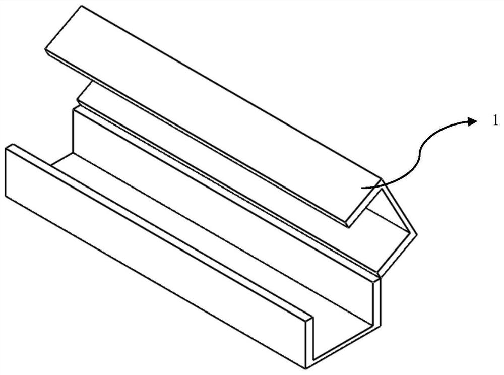
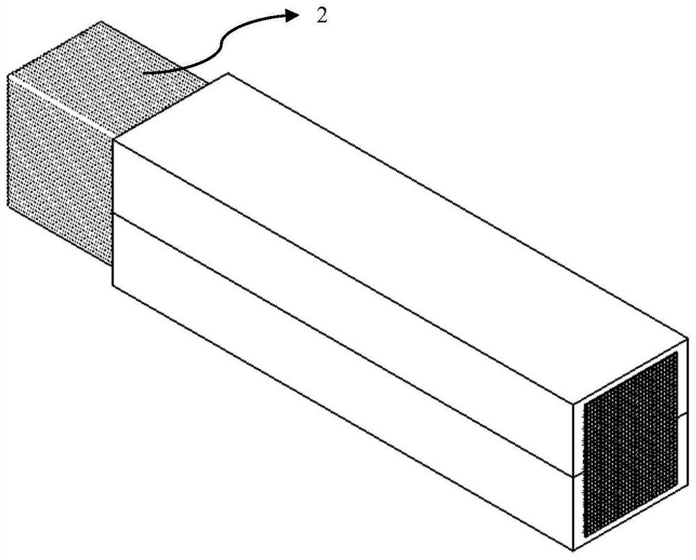
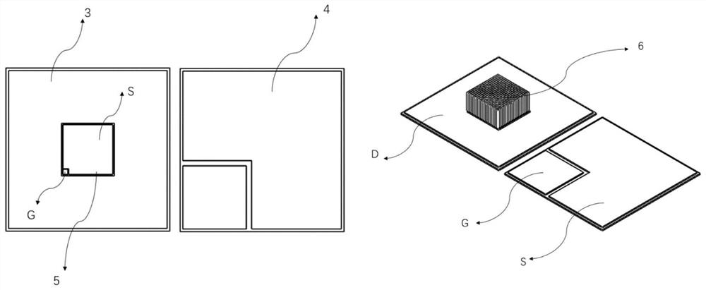
[0017] In view of the above situation, the present invention discloses a preparation method of a copper column spacer based on insulated copper wire that can realize stress buffering and anisotropic conductivity. The new copper column spacer can be used for double-sided heat dissipation / planar electronic devices and modules The encapsulation of several insulated copper wires with a diameter of about 0.3 ~ 0.5mm is bonded together with an epoxy resin polymer adhesive to form a copper wire of a specific shape, and then the copper wire is processed to the required height to replace the Metal posts in double-sided modules.

[0018] Technical scheme of the present invention is as follows:

[0019] The invention discloses a preparation method of a copper column cushion block capable of realizing stress buffering and anisotropic conduction based on insulated copper wires; several insulated copper wires with a diameter of about 0.3 to 0.5 mm are put into a circular or square half-open...


PUM

PropertyMeasurementUnit
diameteraaaaaaaaaa

Abstract

The invention relates to the technical field of packaging of power electronic devices, and aims to propose a new copper pillar spacer technical scheme that can be used for packaging of double-sided heat dissipation / planar electronic devices and modules, so as to realize stress buffering and anisotropic conduction. For this reason, the technical scheme that the present invention adopts is, has the stress cushioning and the copper pillar spacer production method of anisotropy conduction, puts some insulated copper wires that are 0.3~0.5mm in diameter into circular or square semi-open mould, When putting the insulated copper wire into the mold, make the insulated copper wire exceed the length of the front and rear ends of the mold, and the length beyond the front end of the mold must be greater than or equal to the length of the mold itself; Close the mold, put the insulated copper wire beyond the front end of the mold into the polymer adhesive, so that the surface of the insulated copper wire and the interval between every two insulated copper wires are attached with the adhesive. The invention is mainly applied to the packaging occasions of power electronic devices.

Description

technical field [0001] The invention relates to the technical field of packaging of power electronic devices, in particular to a copper pillar spacer with stress buffering and anisotropic conduction and a preparation method thereof. Background technique [0002] With the development of power electronics technology, electronic devices are developing in the direction of high frequency, high density, high power and high temperature applications. The heat dissipation efficiency of the single-sided packaging structure used in traditional semiconductor power devices is not high, and the heat generated inside can only be discharged from the lower surface of the semiconductor power chip. In recent years, the double-sided packaging structure has received more and more attention because it can greatly improve the heat dissipation efficiency of semiconductor power devices. The encapsulation structure can discharge the heat generated inside the semiconductor power device from two direc...

Claims


Application Information

Patent Timeline
Patent Type & Authority Patents(China)
IPC IPC(8): H01L21/60H01L23/488
CPCH01L24/11H01L24/13H01L2224/1111H01L2224/13076
Inventor 梅云辉李靖李欣陆国权
Owner TIANJIN UNIV
Why Eureka
Try Eureka