Manufacturing method of semiconductor device

A manufacturing method and semiconductor technology, applied in the direction of semiconductor/solid-state device manufacturing, semiconductor devices, electric solid-state devices, etc., can solve the problems such as the decline in the yield of multi-layer stacked chips and the increase in the number of semiconductor chips used

Active Publication Date: 2014-10-01
KIOXIA CORP
View PDF7 Cites 1 Cited by
  • Summary
  • Abstract
  • Description
  • Claims
  • Application Information

AI Technical Summary

Problems solved by technology

This is the main reason for the increase in the number of semiconductor chips used and the decline in the manufacturing yield of multilayer stacked chips

Method used


Image

  • Manufacturing method of semiconductor device
  • Manufacturing method of semiconductor device
  • Manufacturing method of semiconductor device

Examples


Embodiment Construction

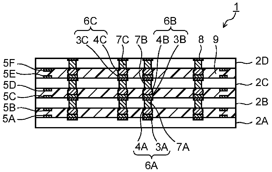
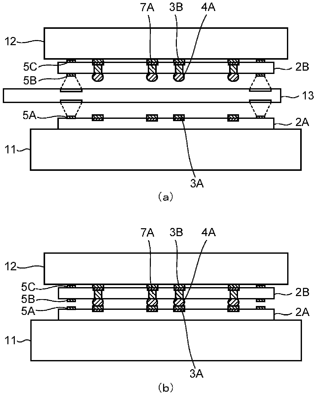
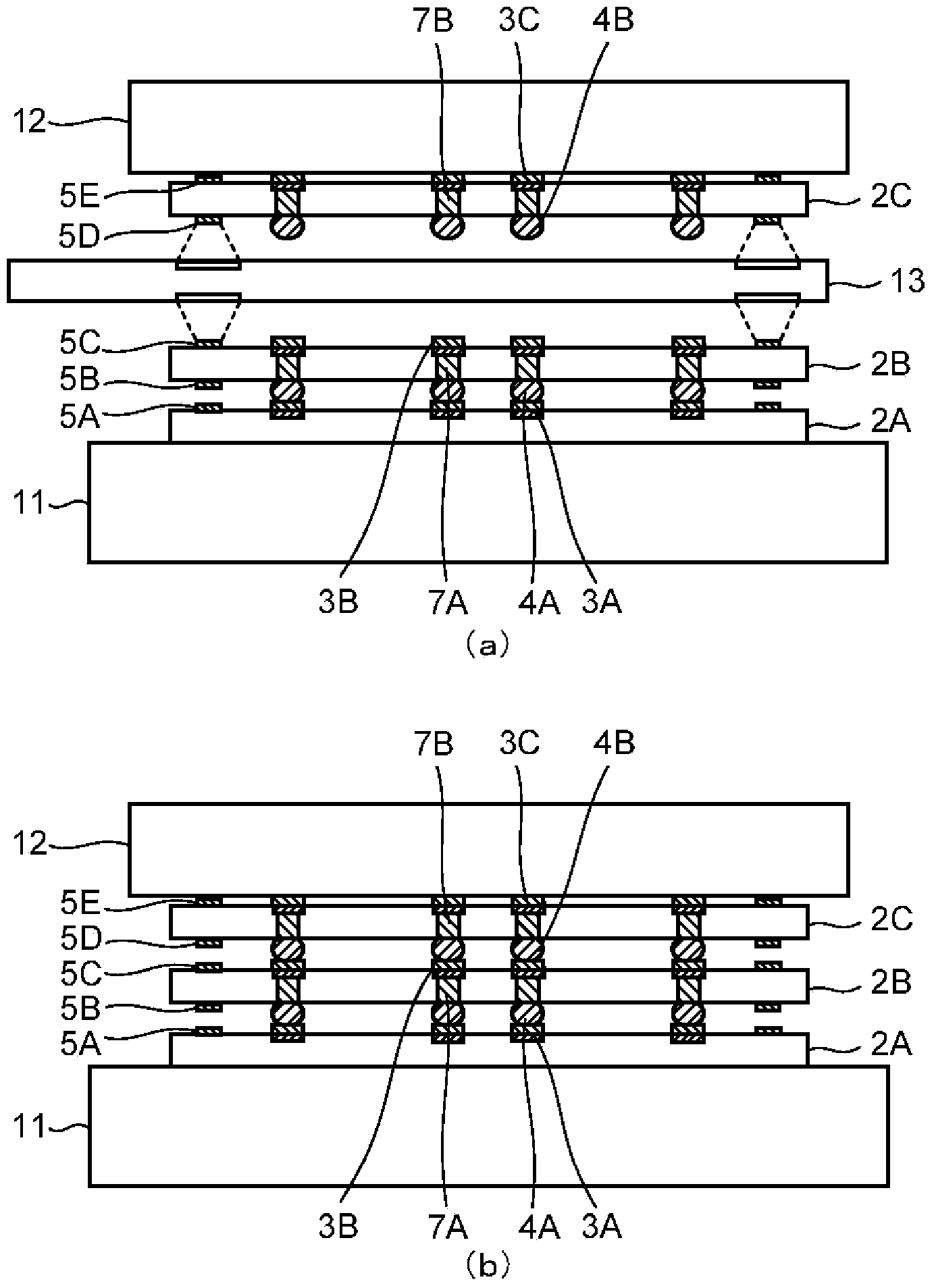
[0014] Next, a method of manufacturing a semiconductor device according to the embodiment will be described with reference to the drawings. First, refer to figure 1 A semiconductor device manufactured using the manufacturing method of the embodiment will be described. figure 1 The illustrated semiconductor device 1 includes a first semiconductor chip 2A, a second semiconductor chip 2B, a third semiconductor chip 2C, and a fourth semiconductor chip 2D. The second to fourth semiconductor chips 2B to 2D are sequentially stacked on the first semiconductor chip 2A. Here, although the semiconductor device 1 in which four semiconductor chips 2 are stacked is illustrated, the number of stacked semiconductor chips 2 is not limited thereto. The number of semiconductor chips 2 constituting the semiconductor device 1 (the number of stacks) may be three or more, and may be three or five or more.

[0015] On the upper surface (first surface) of the first semiconductor chip 2A, first bump...


PUM


Abstract

The invention provides a manufacturing method of a semiconductor device, which can suppress position offset between semiconductor chips when projected electrodes used between the semiconductor chips are connected and laminated. In the manufacturing method of the semiconductor device according to an embodiment, position information of a third aligning mark (5C) of a second semiconductor chip (2B) which is laminated on a first semiconductor chip (2A) and a fourth aligning mark (5D) of a third semiconductor chip (2C) that moves to a second semiconductor chip (4B) is obtained. The second semiconductor chip (2B) and the third semiconductor chip (2C) are aligned and laminated based on the position information of a first aligning mark (5A) arranged on the first semiconductor chip (2A) and the third aligning mark (5C) and the fourth aligning mark (5D).

Description

[0001] This application is based on Japanese Patent Application No. 2013-61230 (filing date: March 25, 2013) and enjoys the priority thereof. This application incorporates this prior application in its entirety by reference. technical field [0002] The present invention relates to a method of manufacturing a semiconductor device. Background technique [0003] In order to achieve miniaturization and high performance of semiconductor devices, stacked semiconductor devices in which a plurality of semiconductor chips are stacked and sealed in one package are being put into practical use. In a stacked semiconductor device, it is necessary to transmit and receive electrical signals between semiconductor chips at high speed. In this case, micro bumps are used for electrical connection between semiconductor chips. The microbumps have a diameter of, for example, about 5 to 50 μm, and are formed on the surface of the semiconductor chip at a pitch of about 10 to 100 μm. In the case ...

Claims


Application Information

Patent Timeline
IPC IPC(8): H01L21/60H01L21/68
CPCH01L2924/15311H01L2224/73257H01L2224/48091H01L2224/16225H01L2224/16145H01L2224/73204H01L2224/32145H01L2224/48227H01L2224/32225H01L24/81H01L2224/8113H01L2924/00014H01L2924/00
Inventor 筑山慧至福田昌利
Owner KIOXIA CORP
Why Eureka
Try Eureka