Array substrate and display device

A technology for array substrates and material layers, applied in instruments, semiconductor devices, optics, etc., can solve the problems of reduced display quality, large spacing, and reduced storage capacitance, and achieve improved pixel aperture ratio, improved display quality, and increased storage capacitance Effect

Active Publication Date: 2014-10-08
BOE TECH GRP CO LTD +1
View PDF4 Cites 21 Cited by
  • Summary
  • Abstract
  • Description
  • Claims
  • Application Information

AI Technical Summary

Problems solved by technology

[0004] Since the size of the capacitor is inversely proportional to the distance between the two plates forming the capacitor, and the color filter layer 108 is generally required to be thicker, the pixel electrode 110 of the array substrate integrated with the color filter layer 108 in the prior art The distance between the common electrode and the common electrode is large, resulting in a reduction in storage capacitance, which cannot meet the leakage current requirements in the display cycle and reduces the stability of the display
[0005] Moreover, since the via hole electrically connecting the pixel electrode 110 and the drain electrode 106 needs to pass through the thick color filter layer 108, the depth of the via hole is extremely large, and the shape of the via hole is difficult to control, which can easily cause the aperture ratio of the via hole to increase. Too large, which will cause the pixel aperture ratio to decrease
On the other hand, the slope angle of the inner wall of the deeper via hole is too steep, which can easily cause the pixel electrode 110 mounted on it to break, reducing the display quality.

Method used


Image

  • Array substrate and display device
  • Array substrate and display device
  • Array substrate and display device

Examples


Embodiment 1

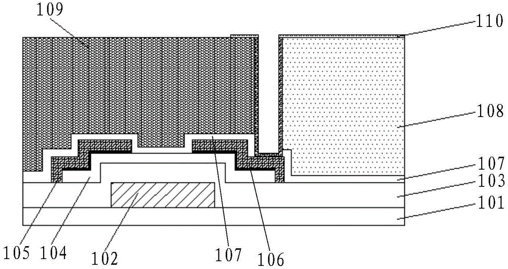
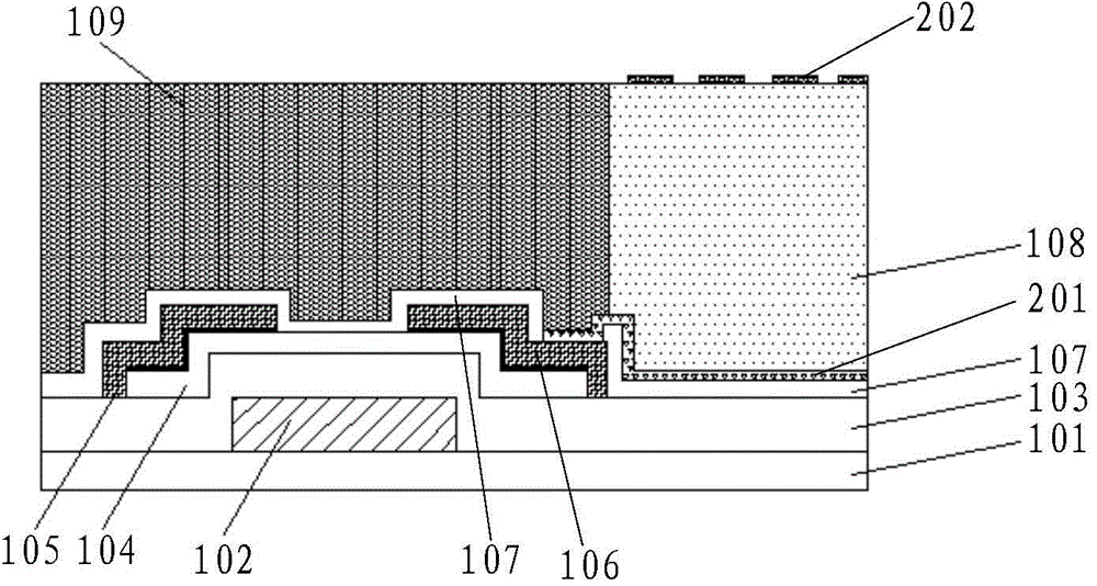
[0038] This embodiment provides an array substrate, including: a thin film transistor, a pixel electrode, and a common electrode; the array substrate further includes: a first material layer located on the thin film transistor, and a first via hole is located in the first material layer; The conductive interlayer on the first material layer, the conductive interlayer is electrically connected to the drain of the thin film transistor through the first via hole; the second material layer located on the conductive interlayer, the second material layer has a structure interconnected with the first via hole The second via hole is staggered, the pixel electrode is located on the second material layer, and the conductive interlayer is electrically connected to the pixel electrode through the second via hole to form a storage capacitor with the common electrode; wherein, the first material layer located on the array substrate The material of the part in the opening area and the materia...

Embodiment 2

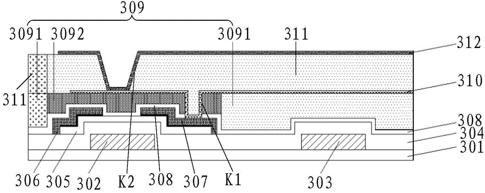
[0064]This embodiment provides an array substrate, including: a thin film transistor, a pixel electrode, and an element for providing a common electrode voltage; the array substrate also includes: a first material layer located on the thin film transistor, and the first material layer has The first via hole; the first conductive interlayer and the second conductive interlayer insulated on the first material layer, the first conductive interlayer is electrically connected to the drain of the thin film transistor through the first via hole, and the second conductive interlayer is connected to the drain of the thin film transistor. The components used to provide the common electrode voltage are electrically connected; the second material layer located on the first conductive interlayer and the second conductive interlayer has a second via hole that is staggered from the first via hole on the second material layer , the pixel electrode is located on the second material layer, the f...

Embodiment 3

[0090] This embodiment provides a display device, which includes the array substrate as described in Embodiment 1 and Embodiment 2. The display device may be any product or component with a display function such as a liquid crystal panel, an electronic paper, an OLED panel, a liquid crystal TV, a liquid crystal display, a digital photo frame, a mobile phone, and a tablet computer. Based on the advantages of the array substrates described in Embodiment 1 and Embodiment 2 above, the display device provided in this embodiment has the advantages of high screen display stability, large pixel aperture ratio, and good display quality compared with the display devices in the prior art. etc., and the display device provided by this embodiment can be of FFS type structure.


PUM


Abstract

The invention provides an array substrate and a display device. The array substrate comprises a first material layer located on a thin film transistor, a conductive sandwich layer located on the first material layer and a second material layer located on the conductive sandwich layer. The first material layer is provided with a first via hole. The conductive sandwich layer is electrically connected with the drain of the thin film transistor through the first via hole. The second material layer is provided with second via hole staggered with first via hole. A pixel electrode is located on the second material layer. The conductive sandwich layer is electrically connected with the pixel electrode through the second via hole so as to form a storage capacitor along with a public electrode. Part of material, located in the opening area of the array substrate, of the first material layer and part of material, located in the opening area of the array substrate, of the second material layer are color photo-resistors. The array substrate and the display device has the advantages that storage capacitance is increased, and display stability, pixel aperture rate and display quality are increased.

Description

technical field [0001] The present invention relates to the field of display technology, in particular to an array substrate and a display device. Background technique [0002] COA (Color-filter on Array) technology is an integrated technology that directly manufactures the color filter layer on the array substrate, which can effectively solve the problems of light leakage caused by alignment deviation in the cell alignment process of liquid crystal display devices, and can significantly Increase the display aperture ratio. [0003] The structure of the array substrate using COA technology in the prior art can be as follows figure 1 As shown, it includes: substrate 101, gate line layer (including gate line, gate 102, common electrode), gate insulating layer 103, semiconductor layer 104, data line layer (including data line, source 105 and drain 106), an insulating layer 107, a color filter layer 108, a light shielding layer 109 and a pixel electrode 110. Wherein, the mate...

Claims


Application Information

Patent Timeline
Patent Type & Authority Applications(China)
IPC IPC(8): G02F1/1362G02F1/1368H01L27/12
CPCH01L27/1248H01L27/1255H01L29/78633H01L27/1214H01L29/42384H01L29/4908
Inventor 李坤
Owner BOE TECH GRP CO LTD
Why Eureka
Try Eureka