Array substrate, manufacturing method of array substrate and display panel of array substrate

An array substrate and a substrate technology are applied in the fields of array substrates and their manufacturing methods and display panels, which can solve the problems of uneven color of displays and different gap sizes of display panels, so as to avoid uneven colors, improve the qualification rate and reduce production. cost effect

Active Publication Date: 2014-10-08
BOE TECH GRP CO LTD +1
View PDF5 Cites 7 Cited by
  • Summary
  • Abstract
  • Description
  • Claims
  • Application Information

AI Technical Summary

Problems solved by technology

[0004] Embodiments of the present invention provide an array substrate, a manufacturing method thereof, and a display panel, which solves the problem that the spacer corresponds to the un

Method used


Image

  • Array substrate, manufacturing method of array substrate and display panel of array substrate
  • Array substrate, manufacturing method of array substrate and display panel of array substrate
  • Array substrate, manufacturing method of array substrate and display panel of array substrate

Examples


Example Embodiment

[0042] The technical solutions in the embodiments of the present invention will be clearly and completely described below in conjunction with the accompanying drawings in the embodiments of the present invention. Obviously, the described embodiments are only a part of the embodiments of the present invention, rather than all the embodiments. Based on the embodiments of the present invention, all other embodiments obtained by those of ordinary skill in the art without creative work shall fall within the protection scope of the present invention.
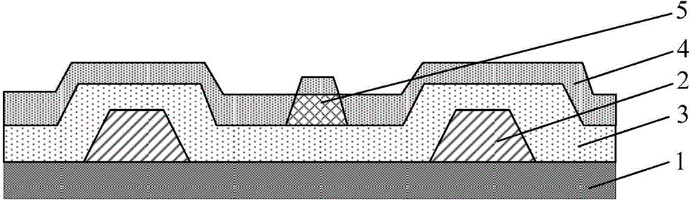
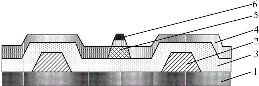
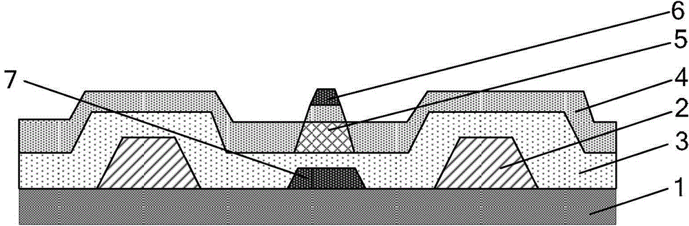
[0043] The embodiment of the present invention provides an array substrate, refer to figure 1 As shown, the array substrate includes: a substrate 1, a gate line 2, a gate insulating layer 3 and a data line (not shown in the figure), wherein:

[0044] When the spacer is arranged at a position corresponding to the gate line and is also arranged at a position corresponding to the data line, the gate line of the array substrate is provided with...


PUM


Abstract

The embodiment of the invention provides an array substrate, a manufacturing method of the array substrate and a display panel of the array substrate and relates to the technical field of display. The problem that an existing display panel is uneven in thickness of a partition pad corresponding to a grid line and/on a data line of the array substrate to cause different gaps after the display panel is boxed is solved. Furthermore, uneven color of a displayer is avoided, and the production cost is reduced. The array substrate comprises a substrate body, the grid line, a grid insulation layer and the data line. Through holes are formed in the grid line and/or the data line of the array substrate and at the positions corresponding to the partition pad. The array substrate is applied to manufacturing of displayers.

Description

technical field [0001] The present invention relates to the field of display technology, in particular to an array substrate, a manufacturing method thereof, and a display panel. Background technique [0002] In the existing technical solution, in the preparation process of the thin film transistor liquid crystal display (Thin Film Transistor Liquid Crystal Display, referred to as TFT-LCD) panel, the gate line and the data line are generally formed by sputtering equipment. However, due to the structural defect of the sputter device itself, there is a problem of inhomogeneity in the film thickness of the gate lines and data lines finally formed by the sputter device. [0003] During the formation of TFT-LCD panels, spacers need to be formed between the array substrate and the color filter substrate. The spacers in the existing technical solutions are generally made at the corresponding positions of the gate lines and / or data lines on the array substrate. at. Due to the non-...

Claims


Application Information

Patent Timeline
IPC IPC(8): H01L27/12H01L21/77G02F1/1368
CPCH01L27/124H01L29/7869
Inventor 郤玉生胡海琛田明
Owner BOE TECH GRP CO LTD
Why Eureka
Try Eureka