
Driving method for liquid crystal device, liquid crystal device, and electronic device

A technology of a liquid crystal device and a driving method, applied in circuits, electrical components, instruments, etc., can solve problems such as light leakage

Inactive Publication Date: 2014-10-15
SEIKO EPSON CORP
View PDF6 Cites 17 Cited by
  • Summary
  • Abstract
  • Description
  • Claims
  • Application Information

AI Technical Summary

Problems solved by technology

When the alignment state of the liquid crystal molecules is changed by the voltage applied between the first electrode and the second electrode of the ion trapping part, sometimes due to the assembly position accuracy of the first substrate and the second substrate, it may be seen that The light leakage caused by the change of the alignment state of the liquid crystal molecules generated by the

Method used


Image

  • Driving method for liquid crystal device, liquid crystal device, and electronic device
  • Driving method for liquid crystal device, liquid crystal device, and electronic device
  • Driving method for liquid crystal device, liquid crystal device, and electronic device

Examples


no. 1 Embodiment approach

[0064] In this embodiment, an active matrix liquid crystal device including a thin film transistor (Thin Film Transistor; TFT) as a switching element of a pixel will be described as an example. This liquid crystal device is a liquid crystal device that can be suitably used as, for example, a light modulation element (liquid crystal light valve) of a projection display device (liquid crystal projector) described later.

[0065] LCD device

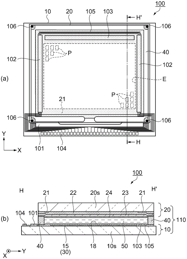
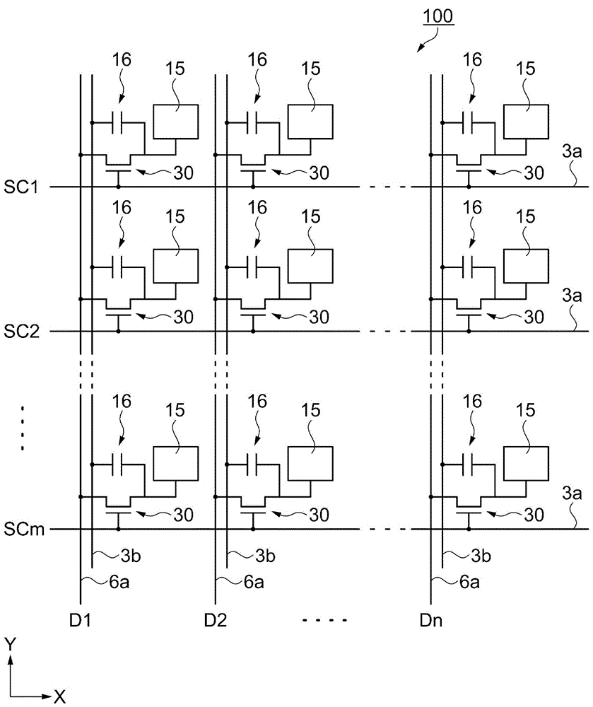
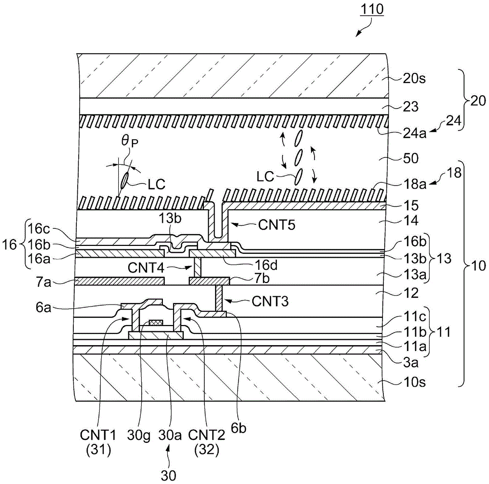
[0066] First, refer to figure 1 and figure 2 The liquid crystal device of this embodiment will be described. figure 1 (a) is a schematic plan view showing the structure of the liquid crystal device of the first embodiment, figure 1 (b) is along figure 1 (a) Schematic cross-sectional view along line H-H'. figure 2 It is an equivalent circuit diagram showing the electrical configuration of the liquid crystal device of the first embodiment.

[0067] Such as figure 1 As shown in (a) and (b), the liquid crystal device 100 of the present ...

no. 2 Embodiment approach

[0137] Next, refer to Figure 8 and Figure 9 The liquid crystal device of the second embodiment will be described. Figure 8 is a wiring diagram showing the structure of the electron partition in the liquid crystal device of the second embodiment, Figure 9 It is a schematic cross-sectional view showing the structure of the liquid crystal device of the second embodiment. The liquid crystal device of the second embodiment differs from the liquid crystal device 100 of the first embodiment in the arrangement of the dummy pixels DP. Therefore, the same reference numerals are assigned to the same configurations as those of the liquid crystal device 100 of the first embodiment, and detailed descriptions are omitted, and the parts different from those of the liquid crystal device 100 of the first embodiment will be described.

[0138] The optical design of the normally black mode is applied to the liquid crystal device 200 of the present embodiment. Such as Figure 8 As shown, ...

no. 3 Embodiment approach )

[0152] Next, refer to Figure 10 and Figure 11 The liquid crystal device of the third embodiment will be described. Figure 10 It is a schematic plan view showing the pixel structure in the liquid crystal device of the third embodiment, Figure 11 It is a schematic cross-sectional view showing the structure of the electron partition in the liquid crystal device of the third embodiment. also, Figure 11 is the same as the first embodiment Figure 6 Corresponding schematic sectional view.

[0153] The liquid crystal device of the third embodiment differs in the structure of the pixel P from the liquid crystal device 100 of the first embodiment. Therefore, the same reference numerals are assigned to the same configurations as those of the liquid crystal device 100 of the first embodiment, and detailed description thereof will be omitted.

[0154] The liquid crystal device 300 of this embodiment employs an optical design in a normally black mode. Such as Figure 10 As sho...


PUM


Abstract

The invention provides a driving method for a liquid crystal device, a liquid crystal device, and an electronic device with the liquid crystal device, which can effectively capture ion impurities in a liquid crystal layer. In the liquid crystal device (100), pixel electrodes (15) and a common electrode (23) that opposes the pixel electrodes (15) on another side of a liquid crystal layer (50) are formed in a display region (E1) serving as a first region, and dummy pixel electrodes (121, 122) serving as first electrodes are formed in a dummy pixel region (E2) serving as a second region. A driving method for the liquid crystal device (100) applies a voltage that is lower than a threshold voltage at which the transmissibility of liquid crystals changes between the dummy pixel electrodes (121, 122) and the common electrode (23). Accordingly, the dummy pixel electrodes (121, 122) can function as an electricity parting portion (120) and ionic impurities can be pulled from the display region (E1) to the dummy pixel electrodes(121, 122).

Description

technical field [0001] The present invention relates to a method of driving a liquid crystal device, a liquid crystal device, and electronic equipment including the liquid crystal device. Background technique [0002] The liquid crystal device includes a liquid crystal panel in which a liquid crystal layer is sandwiched between a pair of substrates. When light enters such a liquid crystal device, the liquid crystal material and / or alignment film constituting the liquid crystal panel may photochemically react with the incident light, and ionic impurities may be generated as reaction products. In addition, it is known that there are ionic impurities diffused into the liquid crystal layer from the sealing material and / or sealing material during the production process of the liquid crystal panel. In particular, in liquid crystal devices used in light modulation units (light valves) of projection display devices (projectors), the beam density of incident light is higher than tha...

Claims


Application Information

Patent Timeline
Patent Type & Authority Applications(China)
IPC IPC(8): G09G3/36G02F1/1343G02F1/1333
CPCG09G2300/0413G02F1/13306G09G2310/0232G09G3/3648G09G2300/0426H01L21/22G09G2300/0876
Inventor 富川直树
Owner SEIKO EPSON CORP
Learn More